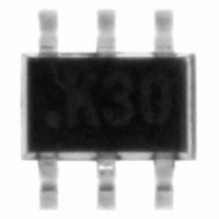
TSH120ICT STMicroelectronics, TSH120ICT Datasheet

TSH120ICT
Specifications of TSH120ICT
TSH120ICT
Available stocks
Related parts for TSH120ICT
TSH120ICT Summary of contents
Page 1
Features ■ Very low consumption ■ Standby mode available ■ Internal reconstruction filter ■ Internal gain of 6dB ■ Rail-to-rail output ■ Tested with +2.5V and +3.3V single supply ■ Operation supply from +2.2V to +5.5V ■ SAG correction ■ ...
Page 2
Absolute maximum ratings 1 Absolute maximum ratings Table 1. Absolute maximum ratings Symbol V Supply voltage CC V Input voltage range in T Operating free air temperature range oper T Storage temperature stg T Maximum junction temperature j R Thermal ...
Page 3
TSH120 2 Electrical characteristics Table 3. Electrical characteristics for V specified) Symbol Parameter DC performance V Output DC level shift dc I Input bias current ib G Internal voltage gain Power supply rejection ratio PSRR 20 log (ΔV /ΔV ) ...
Page 4
Electrical characteristics Table 3. Electrical characteristics for V specified) (continued) Symbol Parameter V Low level output voltage out source ΔG Differential gain Δφ Differential phase Gd Group delay Noise eN Total output noise SNR Output signal to ...
Page 5
TSH120 Figure 1. Frequency response Vcc=+5V -10 Vcc=+3.3V -15 -20 Vcc=+2.5V -25 -30 -35 -40 -45 -50 -55 -60 100k 1M Frequency (Hz) Figure 3. Total input noise vs. frequency 500 400 300 200 100 0 ...
Page 6
Electrical characteristics Figure 6. Quiescent current vs. supply 7.0 6.5 6.0 5.5 5.0 4.5 4.0 2.0 2.5 3.0 3.5 Vcc (V) Figure 8. Standby - Output T Out Out Pin-5 Pin-5 Figure 10. Flatness vs. T amb 0.5 Vout=2Vp-p 0.4 ...
Page 7
TSH120 Figure 12. Voltage gain vs. T 6.10 6.05 6.00 5.95 5.90 5.85 Vcc=+2.5V and +3.3V Ω Load=150 5.80 -40 - Temperature (°C) Figure 14. Supply current vs. T 7.0 6.5 6.0 5.5 5.0 4.5 4.0 Vcc=+2.5V and ...
Page 8
Implementation in the application 3 Implementation in the application This section explains how the TSH120 video buffer operates in a typical application. On the input level shifter optimizes the position of the video signal with no clamping on ...
Page 9
TSH120 4 Power supply considerations Correct power supply bypassing is very important for optimizing performance in the high- frequency range. A bypass capacitor greater than 10μF is necessary to minimize the distortion. For better quality bypassing at higher frequencies, a ...
Page 10
... JEDEC Standard JESD97. The maximum ratings related to soldering conditions are also marked on the inner box label. ECOPACK is an STMicroelectronics trademark. ECOPACK specifications are available at: www.st.com. Figure 22. SC70-6 (or SOT323-6) package footprint (in millimeters) 10/13 0 ...
Page 11
TSH120 Figure 23. SC70-6 (or SOT323-6) package mechanical data Ref Dimensions Millimeters Min Typ Max 0.80 1.10 0 0.10 0.80 1.00 0.15 0.30 0.10 0.18 1.80 2.20 1.15 ...
Page 12
... Ordering information 6 Ordering information Table 4. Order codes Part number TSH120ICT 7 Revision history Table 5. Document revision history Date 29-May-2007 20-Jun-2007 21-Aug-2007 12/13 Temperature Package range SC70-6 -40°C to +85°C (or SOT323-6) Revision 1 Initial version, preliminary data. 2 First complete datasheet. 3 Corrected pinout diagram on cover page (SAG missing). ...
Page 13
... TSH120 Information in this document is provided solely in connection with ST products. STMicroelectronics NV and its subsidiaries (“ST”) reserve the right to make changes, corrections, modifications or improvements, to this document, and the products and services described herein at any time, without notice. All ST products are sold pursuant to ST’s terms and conditions of sale. ...


