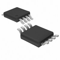
LT1567IMS8#TR Linear Technology, LT1567IMS8#TR Datasheet - Page 3

LT1567IMS8#TR
Manufacturer Part Number
LT1567IMS8#TR
Description
IC BLOCK BUILD FLTR LONOIS 8MSOP
Manufacturer
Linear Technology
Type
General Purposer
Datasheet
1.LT1567CMS8.pdf
(16 pages)
Specifications of LT1567IMS8#TR
Applications
Filter
Mounting Type
Surface Mount
Package / Case
8-MSOP, Micro8™, 8-uMAX, 8-uSOP,
Filter Type
Universal
Order Filter (max)
2nd
Dual Supply Voltage (typ)
±3/±5V
Power Supply Requirement
Single/Dual
Operating Temperature (min)
-40C
Operating Temperature (max)
85C
Lead Free Status / RoHS Status
Contains lead / RoHS non-compliant
ELECTRICAL CHARACTERISTICS
The
values are at T
PARAMETER
OA Input Bias Current
DC BIAS Input Bias Current
OA DC Open-Loop Gain
INV DC Gain
INV DC Input Resistance
OA Gain Bandwidth Product
INV Bandwidth
INV AC Gain
OA Slew Rate
INV Slew Rate
OA Input Voltage Noise Density (Note 7)
OA Input Current Noise Density
Wideband Output Noise for a Second Order Filter (Figure 1)
Total Harmonic Distortion (THD)
for a Second Order Filter (Figure 1)
Output Short-Circuit Current (Note 9)
OA Output Impedance
INV Output Impedance
Note 1: Stresses beyond those listed under Absolute Maximum Ratings
may cause permanent damage to the device. Exposure to any Absolute
Maximum Rating condition for extended periods may affect device
reliability and lifetime.
Note 2: The inputs of each op amp are protected by back-to-back diodes
and diodes to each supply. If either input exceeds the supply or the
differential input voltage exceeds 1.4V, the input current should be limited
to less than 25mA.
Note 3: The LT1567C and LT1567I are guaranteed functional over the
operating temperature range –40°C to 85°C.
Note 4: The LT1567C is guaranteed to meet specified performance from
0°C to 70°C. The LT1567C is designed, characterized and expected to
meet specified performance from –40°C to 85°C but not tested or QA
sampled at these temperatures. The LT1567I is guaranteed to meet
specified performance from – 40°C to 85°C.
●
denotes the specifications that apply over the full operating temperature range (Note 4), otherwise specifications and typical
A
= 25°C. V
S
= ±2.5V, R
L
= 1K, V
OUT
= 0 on both amplifiers unless otherwise noted.
f = 100kHz, OA Connected as
CONDITIONS
V
V
V
V
V
V
V
V
V
Measured at 2MHz, V
Measured at 2MHz, V
Measured at 2MHz, V
–3dB
Measured at 2MHz
V
V
f = 100kHz
f = 100kHz
f
f
f = 1MHz, f
f = 2.5MHz, f
Unity-Gain Inverter
f = 100kHz
C
C
S
S
S
S
S
S
S
S
S
S
S
= 2MHz, BW = 4MHz (Note 8)
= 5MHz, BW = 10MHz (Note 8)
= ±1.5V, R
= ±2.5V, R
= ±2.5V, R
= ±5V, R
= ±1.5V, R
= ±2.5V, R
= ±2.5V, R
= ±5V, R
= ±2.5V, R
= ±5V
= ±5V
C
L
L
= 2MHz, V
C
= 1k, V
= 1k, V
L
L
L
L
L
L
L
= 5MHz, V
= 1k, V
= 1k, V
= 100, V
= 1k, V
= 1k, V
= 100, V
= 1k, V
Note 5: With INVIN pin driven to ±2V.
Note 6: This parameter is not 100% tested.
Note 7: The input referred voltage noise density of the unity gain inverter
is 5.6nV/√Hz which includes the noise of the gain setting resistors.
Note 8: For f
for f
bandwidth of the noise measurement (Figure 1 circuit).
Note 9: Under direct short circuit conditions, with T
current is reduced.
C
O
IN
S
S
S
= 5MHz, C1 = C2 = 180pF, R1 = R2 = 232Ω, R1 = 130Ω. BW is the
= –4V to 4V
O
O
IN
IN
IN
= –4V to 4V
= ±2.5V
= ±1.5V
= ±5V
OUT
= –2V to 2V
O
IN
= –1V to 1V
= –1V to 1V
= –2V to 2V
= –2V to 2V
OUT
= –1.5V to 1.5V
= –1.5V to 1.5V
= 1V
C
= 1V
= 2MHz, C1 = C2 = 180pF, R1 = R2 = 604Ω, R3 = 316Ω and
RMS
RMS
●
●
●
●
●
●
●
●
●
●
●
●
●
●
●
●
0.97
0.97
0.97
0.97
0.96
MIN
450
100
110
120
7.5
1.2
10
10
8
0.03
TYP
–88
–70
600
180
185
190
7.0
1.0
1.4
1.0
0.7
55
60
80
85
55
90
20
30
50
3
6
A
< 25°C the output
LT1567
MAX
1.04
1.04
1.04
1.04
1.05
750
10
15
nV/√Hz
pA/√Hz
µV
µV
UNITS
V/mV
V/mV
V/mV
V/mV
1567fa
3
MHz
MHz
MHz
MHz
V/µs
V/µs
RMS
RMS
V/V
V/V
V/V
V/V
V/V
mA
µA
µA
dB
dB
Ω
Ω
Ω


