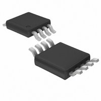
LT1567IMS8#TR Linear Technology, LT1567IMS8#TR Datasheet - Page 10

LT1567IMS8#TR
Manufacturer Part Number
LT1567IMS8#TR
Description
IC BLOCK BUILD FLTR LONOIS 8MSOP
Manufacturer
Linear Technology
Type
General Purposer
Datasheet
1.LT1567CMS8.pdf
(16 pages)
Specifications of LT1567IMS8#TR
Applications
Filter
Mounting Type
Surface Mount
Package / Case
8-MSOP, Micro8™, 8-uMAX, 8-uSOP,
Filter Type
Universal
Order Filter (max)
2nd
Dual Supply Voltage (typ)
±3/±5V
Power Supply Requirement
Single/Dual
Operating Temperature (min)
-40C
Operating Temperature (max)
85C
Lead Free Status / RoHS Status
Contains lead / RoHS non-compliant
LT1567
APPLICATIO S I FOR ATIO
output from the INV block (Pin 7). These two outputs
maintain equal gain and 180º phase shift over a wide
frequency range. This feature permits choosing the signal
polarity in single ended applications, and also performs
single ended to differential conversion. The latter property
is useful as an antialiasing filter to drive standard mono-
lithic A/D converters having differential inputs, as illus-
trated on the first page of this data sheet.
Dealing with High Source Impedances
The voltage V
signal voltage that the filter sees. If a voltage source with
significant internal impedance drives the V
Figure 1, then the filter input V
source’s open-circuit output, and the difference can be
complex, because the filter presents a complex imped-
ance to V
negligibly “low” if it is much smaller than R1 at frequencies
of interest. Otherwise, the source impedance (resistive or
reactive) effectively adds to R1 and may change the signal
frequency response compared to that with a low source
impedance. If the source is resistive and predictable, then
it may be possible to design for it by reducing R1.
Unpredictable or nonresistive source impedances that are
not much less than R1 should be buffered.
Construction and Instrumentation Cautions
Electrically clean construction is important in applica-
tions seeking the full dynamic range and bandwidth of the
LT1567. Using the shortest possible wiring or printed-
circuit paths will minimize parasitic capacitance and
inductance. High quality supply bypass capacitors of
0.1µF near the chip, connected to a ground plane, provide
good decoupling from a clean, low inductance power
source. But several inches of wire (i.e., a few microhenrys
of inductance) from the power supplies, unless decoupled
by substantial capacitance (≥10µF) near the chip, can
10
IN
. A rule of thumb is that a source impedance is
IN
in Figure 1, on the left side of R1, is the
U
U
IN
W
may differ from the
IN
U
node in
cause a high Q LC resonance in the hundreds of kHz in the
chip’s supplies or ground reference. This may impair filter
performance at those frequencies. In stringent filter
applications, a compact, carefully laid out printed circuit
board with good ground plane makes a difference in both
stopband rejection and distortion. Finally, equipment to
measure filter performance can itself introduce distortion
or noise. Checking for these limits with a wire in place of
the filter is a prudent routine procedure.
Low Noise Differential Circuits
The LT1567 is an optimum analog building for designing
single supply differential circuits to process low level
signals. Figure 3 shows a single ended to differential
amplifier driving a 1st order differential RC filter. The
differential output of Figure 3 is a function of input (V
and the V
voltage on Pin 5 in Figures 3, 4 and 5 is the common mode
input voltage range parameter under Electrical
Characteristics.)The graph of Figure 3 shows the differen-
tial signal-to-noise ratio for a gain of 2 and a gain of 10.
Increasing the differential gain increases the differential
signal-to-noise ratio. The equivalent input noise is equal to
the output noise divided by the gain. For example, with a
gain equal to 2 (R2 = R1 = 200Ω) and a gain equal to 10
(R2 = 1k, R1 = 200Ω), the equivalent input noise is 4.59nV/
√Hz and 2.04nV/√Hz respectively. The V
5 can be set by a voltage divider or a reference voltage
source. To maximize the unclipped LT1567 output swing,
the DC output voltage should be set at V
V
then V
be AC coupled to the input resistor, R1, and V
DC voltage of the circuit following the amplifier. For
example, V
I and Q modulator used in broadband communication
systems.
INDC
(the input DC voltage) is within the range of V
REF
can be equal to V
REF
REF
voltage on Pin 5. (The range of the V
might be set to 1.2V to bias the input of an
INDC
. The input signal can also
REF
+
/2. However, if
voltage on Pin
REF
set to the
1567fa
REF
REF
IN
)
,


