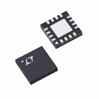
LTC6400CUD-20#PBF Linear Technology, LTC6400CUD-20#PBF Datasheet - Page 13

LTC6400CUD-20#PBF
Manufacturer Part Number
LTC6400CUD-20#PBF
Description
IC ADC DRIVER DIFF 16-QFN
Manufacturer
Linear Technology
Type
ADC Driverr
Datasheet
1.LTC6400CUD-20PBF.pdf
(16 pages)
Specifications of LTC6400CUD-20#PBF
Applications
Data Acquisition
Mounting Type
Surface Mount
Package / Case
16-WQFN Exposed Pad
No. Of Amplifiers
1
Input Offset Voltage
2mV
Gain Db Max
20dB
Bandwidth
1.8GHz
Slew Rate
4.5V/ns
Supply Voltage Range
2.85V To 3.5V
Supply Current
90mA
Amplifier Case Style
QFN
Rohs Compliant
Yes
Lead Free Status / RoHS Status
Lead free / RoHS Compliant
Available stocks
Company
Part Number
Manufacturer
Quantity
Price
APPLICATIONS INFORMATION
1.6V. The bandwidth of V
which is dominated by a low pass fi lter connected to the
V
generation at the outputs. The internal common mode
feedback loop has a –3dB bandwidth around 300MHz,
allowing fast common mode rejection at the outputs of
the LTC6400-20. The V
voltage with a 0.1μF bypass capacitor. When interfacing
with A/D converters such as the LT22xx families, the V
pin can be connected to the V
Driving A/D Converters
The LTC6400-20 has been specifi cally designed to inter-
face directly with high speed A/D converters. In Figure 7,
an example schematic shows the LTC6400-20 with a
single-ended input driving the LTC2208, which is a 16-bit,
130Msps ADC. Two external 10Ω resistors help eliminate
potential resonance associated with stray capacitance of
PCB traces and bond wires of either the ADC input or
the driver output. V
to V
single-ended input signal can be converted to differential
signal via a balun and fed to the input of the LTC6400-20.
The balun also converts input impedance to match 50Ω
source impedance.
Figure 8 summarizes the spurious free dynamic range
(SFDR) for IMD3 of the whole system in Figure 7.
Test Circuits
Due to the fully-differential design of the LTC6400 and
its usefulness in applications with differing characteristic
IF IN
OCM
66.5Ω
Figure 7. Single-Ended Input to LTC6400-20 and LTC2208
CM
29Ω
pin and is aimed to reduce common mode noise
of the LTC2208 V
0.1μF
0.1μF
+IN
–IN
ENABLE
LTC6400-20
OCM
V
OCM
OCM
+OUT
–OUT
of the LTC6400-20 is connected
CM
OCM
+OUTF
–OUTF
20dB GAIN
pin should be tied to a DC bias
pin at 1.25V. Alternatively, a
control is typically 15MHz,
CM
0.1μF
pin of the ADC.
10Ω
10Ω
1.25V
AIN
AIN
LTC2208 130Msps
–
+
LTC2208
16-Bit ADC
V
CM
640020 F07
OCM
specifi cations, two test circuits are used to generate the
information in this datasheet. Test Circuit A is DC987B,
a two-port demonstration circuit for the LTC6400 family.
The schematic and silkscreen are shown below. This
circuit includes input and output transformers (baluns)
for single-ended-to-differential conversion and imped-
ance transformation, allowing direct hook-up to a 2-port
Figure 8. SFDR for the Combination of LTC6400-20 and LTC2208
94
92
90
88
86
84
82
70
120
Top Silkscreen
FREQUENCY (MHz)
170
220
LTC6400-20
270 300
640020 F08
13
640020f


