TFA9800J/N1,112 NXP Semiconductors, TFA9800J/N1,112 Datasheet - Page 7
TFA9800J/N1,112
Manufacturer Part Number
TFA9800J/N1,112
Description
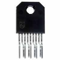
IC AMP AUDIO PWR 7W STER AB 9SIL
Manufacturer
NXP Semiconductors
Type
Class ABr
Datasheet
1.TFA9800JN1112.pdf
(17 pages)
Specifications of TFA9800J/N1,112
Output Type
2-Channel (Stereo)
Package / Case
9-SIL (Bent and Staggered Leads)
Max Output Power X Channels @ Load
7W x 2 @ 4 Ohm
Voltage - Supply
6 V ~ 18 V
Features
Depop, Mute, Short-Circuit and Thermal Protection, Standby
Mounting Type
Through Hole
Product
Class-AB
Output Power
7 W
Available Set Gain
20 dB
Thd Plus Noise
0.1 %
Operating Supply Voltage
15 V
Supply Current
40 mA
Maximum Power Dissipation
25 W
Maximum Operating Temperature
+ 85 C
Mounting Style
Through Hole
Audio Load Resistance
4 Ohms
Input Signal Type
Differential
Minimum Operating Temperature
- 40 C
Output Signal Type
Single
Supply Type
Single
Supply Voltage (max)
18 V
Supply Voltage (min)
6 V
Lead Free Status / RoHS Status
Lead free / RoHS Compliant
Other names
935279697112
TFA9800J
TFA9800J
TFA9800J
TFA9800J


Philips Semiconductors
12. Application information
TFA9800J_1
Preliminary data sheet
12.1 Printed-Circuit Board (PCB) layout and grounding
12.2 Input configuration
12.3 Built-in protection circuits
For high system performance level, certain grounding techniques are imperative. The
input reference grounds have to be tied with their respective source grounds and must
have separate traces from the power ground traces; this will prevent the large (output)
signal currents from interfering with the small AC input signals. The small-signal ground
traces should be physically located as far as possible from the power ground traces. The
width of supply and output traces should be as large as practical for delivering maximum
output power.
Proper supply bypassing is critical for low noise performance and high power supply
rejection. The respective capacitor locations should be as close as possible to the device
and grounded to the power ground. Proper power supply decoupling also prevents
oscillations. For suppressing higher frequency transients (spikes) on the supply line a
capacitor with low Equivalent Series Resistance (ESR), typical 0.1 F, has to be placed as
close as possible to the device. For suppressing lower frequency noise and ripple signals,
a large electrolytic capacitor, e.g. 1000 F or greater, must be placed close to the
TFA9800J.
In a single-ended (stereo) application a bypass capacitor on the SVRR pin reduces the
noise and ripple on the mid-rail voltage. For good THD and noise performance a low ESR
capacitor is recommended.
It should be noted that the DC level of the input pins is about 2.1 V, therefore a coupling
capacitor is necessary.
The input cut-off frequency is:
This calculation shows that it is not necessary to use high capacitor values for the input;
so the delay during switch-on, which is necessary for charging the input capacitors, can
be minimized. This results in a good low frequency response and good switch-on
behavior.
For stereo application (single-ended) coupling capacitors on both input and output are
necessary.
The TFA9800J contains two kinds of protection circuits:
•
•
Short-circuit of outputs to ground, supply and across the load: short-circuit is detected
and controlled by a Safe Operating ARea (SOAR) protection circuit.
Thermal shutdown protection: the junction temperature is measured by a temperature
sensor; at a junction temperature of > 150 C, thermal fold back is activated.
Rev. 01 — 17 March 2006
f
i
=
----------------- -
2 R
1
i
C
i
f
i
=
----------------------------------------------------------------- -
2
30 10
2
© Koninklijke Philips Electronics N.V. 2006. All rights reserved.
7 W stereo power amplifier
1
3
220 10
TFA9800J
9 –
=
24 Hz
7 of 17
Related parts for TFA9800J/N1,112
Image
Part Number
Description
Manufacturer
Datasheet
Request
R

Part Number:
Description:
Tfa9800j 2 X 7 W Stereo Power Amplifier
Manufacturer:
NXP Semiconductors
Datasheet:

Part Number:
Description:
Audio Amplifiers 2X6W AUDIO AMPLIFIER
Manufacturer:
NXP Semiconductors
Datasheet:
Part Number:
Description:
NXP Semiconductors designed the LPC2420/2460 microcontroller around a 16-bit/32-bitARM7TDMI-S CPU core with real-time debug interfaces that include both JTAG andembedded trace
Manufacturer:
NXP Semiconductors
Datasheet:

Part Number:
Description:
NXP Semiconductors designed the LPC2458 microcontroller around a 16-bit/32-bitARM7TDMI-S CPU core with real-time debug interfaces that include both JTAG andembedded trace
Manufacturer:
NXP Semiconductors
Datasheet:
Part Number:
Description:
NXP Semiconductors designed the LPC2468 microcontroller around a 16-bit/32-bitARM7TDMI-S CPU core with real-time debug interfaces that include both JTAG andembedded trace
Manufacturer:
NXP Semiconductors
Datasheet:
Part Number:
Description:
NXP Semiconductors designed the LPC2470 microcontroller, powered by theARM7TDMI-S core, to be a highly integrated microcontroller for a wide range ofapplications that require advanced communications and high quality graphic displays
Manufacturer:
NXP Semiconductors
Datasheet:
Part Number:
Description:
NXP Semiconductors designed the LPC2478 microcontroller, powered by theARM7TDMI-S core, to be a highly integrated microcontroller for a wide range ofapplications that require advanced communications and high quality graphic displays
Manufacturer:
NXP Semiconductors
Datasheet:
Part Number:
Description:
The Philips Semiconductors XA (eXtended Architecture) family of 16-bit single-chip microcontrollers is powerful enough to easily handle the requirements of high performance embedded applications, yet inexpensive enough to compete in the market for hi
Manufacturer:
NXP Semiconductors
Datasheet:
Part Number:
Description:
The XA-S3 device is a member of Philips Semiconductors? XA(eXtended Architecture) family of high performance 16-bitsingle-chip microcontrollers
Manufacturer:
NXP Semiconductors
Datasheet:

Part Number:
Description:
The NXP BlueStreak LH75401/LH75411 family consists of two low-cost 16/32-bit System-on-Chip (SoC) devices
Manufacturer:
NXP Semiconductors
Datasheet:
Part Number:
Description:
The NXP LPC3130/3131 combine an 180 MHz ARM926EJ-S CPU core, high-speed USB2
Manufacturer:
NXP Semiconductors
Datasheet:
Part Number:
Description:
The NXP LPC3141 combine a 270 MHz ARM926EJ-S CPU core, High-speed USB 2
Manufacturer:
NXP Semiconductors
Part Number:
Description:
The NXP LPC3143 combine a 270 MHz ARM926EJ-S CPU core, High-speed USB 2
Manufacturer:
NXP Semiconductors

Part Number:
Description:
The NXP LPC3152 combines an 180 MHz ARM926EJ-S CPU core, High-speed USB 2
Manufacturer:
NXP Semiconductors