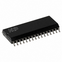
TDA8933T/N1,112 NXP Semiconductors, TDA8933T/N1,112 Datasheet - Page 28

TDA8933T/N1,112
Manufacturer Part Number
TDA8933T/N1,112
Description
IC AMP AUDIO 32W STER D 32SOIC
Manufacturer
NXP Semiconductors
Type
Class Dr
Datasheet
1.TDA8933TN1112.pdf
(47 pages)
Specifications of TDA8933T/N1,112
Output Type
1-Channel (Mono) or 2-Channel (Stereo)
Package / Case
32-SOIC (7.5mm Width)
Max Output Power X Channels @ Load
32W x 1 @ 16 Ohm; 15.7W x 2 @ 8 Ohm
Voltage - Supply
10 V ~ 36 V, ±5 V ~ 18 V
Features
Depop, Differential Inputs, Mute, Short-Circuit and Thermal Protection
Mounting Type
Surface Mount
Product
Class-D
Output Power
32 W
Available Set Gain
36 dB
Common Mode Rejection Ratio (min)
75 dB
Thd Plus Noise
0.011 %
Operating Supply Voltage
25 V
Supply Current
0.6 mA
Maximum Power Dissipation
5000 mW
Maximum Operating Temperature
+ 85 C
Mounting Style
SMD/SMT
Audio Load Resistance
16 Ohms
Dual Supply Voltage
+/- 12.5 V
Input Signal Type
Differential
Minimum Operating Temperature
- 40 C
Output Signal Type
Differential, Single
Supply Type
Single or Dual
Supply Voltage (max)
36 V
Supply Voltage (min)
10 V
Lead Free Status / RoHS Status
Lead free / RoHS Compliant
Other names
935281484112
TDA8933T
TDA8933T
TDA8933T
TDA8933T
NXP Semiconductors
TDA8933_1
Preliminary data sheet
14.6 Device synchronization
Where:
Example:
Substituting R1 = R2 = 4.7 k , Z
results in a gain of G
If two or more TDA8933 devices are used in one application it is recommended that all
devices are synchronized at the same switching frequency to avoid beat tones.
Synchronization can be realized by connecting all OSCIO pins together and configuring
one of the TDA8933 devices as master, while the other TDA8933 devices are configured
as slaves (see
A device is configured as master when a resistor R
and pin V
configured as an oscillator output for synchronization. The OSCREF pins of the slave
devices should be shorted to pin V
R
Fig 10. Master/slave concept in two-chip application
EQ
R1 = series resistors (
R2 = series resistors (
R
R3 = parallel resistor (
Z
i
EQ
= internal input impedance (
=
= equivalent resistance (
----------------- -
R3
R3
SSD(HW)
+
Z
Z
i
i
Figure
100 nF
, setting the carrier frequency. Pin OSCIO of the master is then
C osc
v(tot)
master
10).
OSCREF
Rev. 01 — 15 May 2007
= 26.3 dB.
R osc
39 k
TDA8933
V
SSD(HW)
IC1
i
= 100 k and R3 = 22 k in
SSD(HW)
OSCIO
, configuring pin OSCIO as an input.
slave
osc
OSCIO
is connected between pin OSCREF
TDA8933
V
SSD(HW)
IC2
Equation 8
Class-D audio amplifier
OSCREF
010aaa138
TDA8933
© NXP B.V. 2007. All rights reserved.
and
Equation 9
28 of 47
(9)


