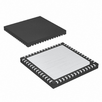
MAX9741ETN+D Maxim Integrated Products, MAX9741ETN+D Datasheet - Page 12

MAX9741ETN+D
Manufacturer Part Number
MAX9741ETN+D
Description
IC AMP AUDIO PWR 12W STER 56TQFN
Manufacturer
Maxim Integrated Products
Type
Class Dr
Datasheet
1.MAX9741ETNTD.pdf
(16 pages)
Specifications of MAX9741ETN+D
Output Type
2-Channel (Stereo)
Max Output Power X Channels @ Load
12W x 2 @ 8 Ohm
Voltage - Supply
10 V ~ 25 V
Features
Depop, Differential Inputs, Mute, Short-Circuit and Thermal Protection, Shutdown
Mounting Type
Surface Mount
Package / Case
56-TQFN
Lead Free Status / RoHS Status
Lead free / RoHS Compliant
12W+12W, Low-EMI, Spread-Spectrum,
Stereo, Class D Amplifier
Audio content, both music and voice, has a much lower
RMS value relative to its peak output power.
shows a sine wave and an audio signal in the time
domain. Both are measured for RMS value by the oscil-
loscope. Although the audio signal has a slightly higher
peak value than the sine wave, its RMS value is almost
half that of the sine wave. Therefore, while an audio sig-
nal may reach similar peaks as a continuous sine wave,
the actual thermal impact on the Class D amplifier is
highly reduced. If the thermal performance of a system
is being evaluated, it is important to use actual audio
signals instead of sine waves for testing. If sine waves
must be used, the thermal performance will be less
than the system’s actual capability.
The exposed pad is the primary route of heat away
from the IC. With a bottom-side exposed pad, the PC
board and its copper becomes the primary heatsink for
the Class D amplifier. Solder the exposed pad to a
large copper polygon. Add as much copper as possi-
ble from this polygon to any adjacent pin on the Class
D amplifier as well as to any adjacent components, pro-
vided these connections are at the same potential.
These copper paths must be as wide as possible. Each
of these paths contributes to the overall thermal capa-
bilities of the system.
The copper polygon to which the exposed pad is
attached should have multiple vias to the opposite side
of the PC board, where they connect to another copper
polygon. Make this polygon as large as possible within
the system’s constraints for signal routing.
Additional improvements are possible if all the traces
from the device are made as wide as possible.
Although the IC pins are not the primary thermal path
out of the package, they do provide a small amount.
The total improvement would not exceed approximately
10%, but it could make the difference between accept-
able performance and thermal problems.
With a bottomside exposed pad, the lowest resistance
thermal path is on the bottom of the PC board. The topside
of the IC is not a significant thermal path for the device.
The die temperature of a Class D amplifier can be esti-
mated with some basic calculations. For example, the
die temperature is calculated for the below conditions:
• T
• P
• Efficiency (η) = 78%
• θ
12
JA
A
OUT
______________________________________________________________________________________
= +40°C
= 21°C/W
= 10W (5W + 5W)
PC Board Thermal Considerations
Thermal Calculations
Figure 5
First, the Class D amplifier’s power dissipation must be
calculated.
Then the power dissipation is used to calculate the die
temperature, T
The on-resistance of the MOSFET output stage in Class
D amplifiers affects both the efficiency and the peak-
current capability. Reducing the peak current into the
load reduces the I
ing efficiency. To keep the peak currents lower, choose
the highest impedance speaker which can still deliver
the desired output power within the voltage swing limits
of the Class D amplifier and its supply voltage.
To optimize efficiency, load the output stage with 12Ω
to 16Ω speakers. The MAX9741 exhibits highest effi-
ciency performance when driving higher load imped-
ance (see the Typical Operating Characteristics). If a
12Ω to 16Ω load is not available, select a lower supply
voltage when driving 4Ω to 10Ω loads.
For best performance, choose a speaker impedance to
complement the required output power and the available
supply voltage. For example, if operating from a 24V sup-
ply and a peak output of 10W per channel is desired, using
12Ω speakers provides the best audio performance and
power efficiency. The amplifier outputs are short-circuit
protected at approximately 2A. Selecting a higher imped-
ance driver helps prevent exceeding the current limit.
Figure 5. RMS Comparison of Sine Wave vs. Audio Signal
T
C
=
T
P
A
DISS
Load Impedance and Supply Voltage
+
P
Optimize MAX9741 Efficiency with
DISS
=
C
P
OUT
, as follows:
×
η
θ
2
JA
R losses in the MOSFETs, increas-
−
P
=
OUT
40
20ms/div
° +
C
=
10
78
2 82
.
W
%
Load Impedance
W
−
10
×
21
W
°
=
C W
2 82
/
.
=
W
99 2
.
°
C


