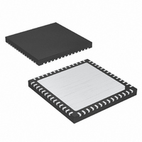
MAX9741ETN+D Maxim Integrated Products, MAX9741ETN+D Datasheet - Page 11

MAX9741ETN+D
Manufacturer Part Number
MAX9741ETN+D
Description
IC AMP AUDIO PWR 12W STER 56TQFN
Manufacturer
Maxim Integrated Products
Type
Class Dr
Datasheet
1.MAX9741ETNTD.pdf
(16 pages)
Specifications of MAX9741ETN+D
Output Type
2-Channel (Stereo)
Max Output Power X Channels @ Load
12W x 2 @ 8 Ohm
Voltage - Supply
10 V ~ 25 V
Features
Depop, Differential Inputs, Mute, Short-Circuit and Thermal Protection, Shutdown
Mounting Type
Surface Mount
Package / Case
56-TQFN
Lead Free Status / RoHS Status
Lead free / RoHS Compliant
The MAX9741 can be configured as single-ended input
amplifiers by capacitively coupling either input to GND
and driving the other input
An input capacitor, C
impedance of the MAX9741, forms a highpass filter that
removes the DC bias from an incoming signal. The AC-
coupling capacitor allows the amplifier to bias the sig-
nal to an optimum DC level. Assuming zero-source
impedance, the -3dB point of the highpass filter is
given by:
Choose C
of interest. Setting f
quency response of the amplifier. Use capacitors with
dielectrics that have low-voltage coefficients, such as
tantalum or aluminum electrolytic. Capacitors with high-
voltage coefficients, such as ceramics, may result in
increased distortion at low frequencies.
Use capacitors with an ESR less than 100mΩ for opti-
mum performance. Low-ESR ceramic capacitors mini-
mize the output resistance of the charge pump. For
best performance over the extended temperature
range, select capacitors with an X7R dielectric.
The value of the flying capacitor (C1) affects the load
regulation and output resistance of the charge pump. A
C1 value that is too small degrades the device’s ability
to provide sufficient current drive. Increasing the value
of C1 improves load regulation and reduces the
charge-pump output resistance to an extent. Above
1µF, the on-resistance of the switches and the ESR of
C1 and C2 dominate.
The output capacitor value and ESR directly affect the rip-
ple at CHOLD. Increasing C2 reduces output ripple.
Likewise, decreasing the ESR of C2 reduces both ripple
and output resistance. Lower capacitance values can be
used in systems with low maximum output power levels.
In certain systems, a single audio source can be shared
by multiple devices (speaker and headphone amplifiers).
IN
Charge-Pump Capacitor Selection
so f
-3dB
f
______________________________________________________________________________________
- 3dB
-3dB
is well below the lowest frequency
IN
12W+12W, Low-EMI, Spread-Spectrum,
=
, in conjunction with the input
2
too high affects the low-fre-
(Figure
π
Sharing Input Sources
Component Selection
R
IN
1
Flying Capacitor (C1)
C
4).
Hold Capacitor (C2)
Single-Ended Input
IN
Input Filter
Stereo, Class D Amplifier
When sharing inputs, it is common to mute the unused
device, rather than completely shutting it down, prevent-
ing the unused device inputs from distorting the input
signal. Mute the MAX9741 by driving SS low through an
open-drain output or MOSFET. Driving SS low turns off
the Class D output stage, but does not affect the input
bias levels of the MAX9741. Be aware that during normal
operation, the voltage at SS can be up to 7V, depending
on the MAX9741 supply.
Proper power-supply bypassing ensures low-distortion
operation. For optimum performance, bypass V
PGND with a 0.1µF or greater capacitor as close to each
V
capacitor in parallel with a larger value, low-ESR ceramic
or aluminum electrolytic capacitor provides good results.
A low-impedance, high-current power-supply connection
to V
be added as required depending on the application and
power-supply characteristics. AGND and PGND should
be star connected to system ground. Refer to the
MAX9741 Evaluation Kit for layout guidance.
Class D amplifiers provide much better efficiency and
thermal performance than a comparable Class AB
amplifier. However, the system’s thermal performance
must be considered with realistic expectations and
consideration of many parameters. This application
note examines Class D amplifiers using general exam-
ples to illustrate good design practices.
When a Class D amplifier is evaluated in the lab, often
a continuous sine wave is used as the signal source.
While this is convenient for measurement purposes, it
represents a worst-case scenario for thermal loading
on the amplifier. It is not uncommon for a Class D
amplifier to enter thermal shutdown if driven near maxi-
mum output power with a continuous sine wave.
Figure 4. Single-Ended Input
DD
Class D Amplifier Thermal Considerations
DD
pin as possible. In some applications, a 0.1µF
is assumed. Additional bulk capacitance should
SINGLE-ENDED
AUDIO INPUT
0.47µF
Continuous Sine Wave vs. Music
0.47µF
Supply Bypassing/Layout
IN+
IN-
MAX9741
DD
11
to


