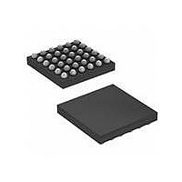
MAX97000EWA+T Maxim Integrated Products, MAX97000EWA+T Datasheet - Page 17

MAX97000EWA+T
Manufacturer Part Number
MAX97000EWA+T
Description
IC AUDIO SUBSYSTEM 25WLP
Manufacturer
Maxim Integrated Products
Series
DirectDrive™r
Type
Class Dr
Datasheet
1.MAX97000EWAT.pdf
(34 pages)
Specifications of MAX97000EWA+T
Output Type
1-Channel (Mono) with Stereo Headphones
Max Output Power X Channels @ Load
930mW x 1 @ 8 Ohm; 40mW x 2 @ 16 Ohm
Voltage - Supply
2.7 V ~ 5.5 V
Features
Depop, Differential Inputs, I²C, Mute, Shutdown, Volume Control
Mounting Type
Surface Mount
Package / Case
25-WLP
Product
Class-D
Output Power
725 mW
Available Set Gain
12 dB
Common Mode Rejection Ratio (min)
32 dB to 55 dB
Thd Plus Noise
0.05 %
Operating Supply Voltage
2.7 V to 5.5 V
Supply Current
0.4 mA to 1.45 mA
Maximum Power Dissipation
850 mW
Maximum Operating Temperature
+ 80 C
Mounting Style
SMD/SMT
Audio Load Resistance
41.2 KOhms
Input Signal Type
Differential
Minimum Operating Temperature
- 40 C
Output Signal Type
Differential
Supply Voltage (max)
5.5 V
Supply Voltage (min)
2.7 V
Lead Free Status / RoHS Status
Lead free / RoHS Compliant
Other names
MAX97000EWA+T
BUMP
A1
A2
A3
A4
A5
B1
B2
B3
B4
B5
C1
C2
C3
C4
C5
Speaker and Class H Headphone Amplifier
HPVDD
HPVSS
LDOIN
NAME
PGND
SHDN
PVDD
GND
BIAS
VDD
C1P
C1N
HPR
SDA
SCL
HPL
Audio Subsystem with Mono Class D
Charge-Pump Flying Capacitor Positive Terminal. Connect a 1FF capacitor between C1P and
C1N.
Charge-Pump Flying Capacitor Negative Terminal. Connect a 1FF capacitor between C1P and
C1N.
Headphone Amplifier Positive Power Supply. Bypass with a 1FF capacitor to PGND.
Headphone Amplifier Negative Power Supply. Bypass with a 1FF capacitor to PGND.
Headphone Amplifier Right Output
LDO Output and Headphone Amplifier Supply. Bypass with a 1FF and a 10FF capacitor to
GND. Power VDD or LDOIN. When powering VDD, leave LDOIN unconnected.
LDO Input. Generates VDD if no 1.8V power supply is available. Leave unconnected to disable.
Do not power VDD when powering LDOIN.
Serial Data Input/Output. Connect a pullup resistor from SDA to the I
Serial-Clock Input. Connect a pullup resistor from SCL to the I
Headphone Amplifier Left Output
Class D Power Supply. Bypass with a 1FF and a 10FF capacitor to PGND.
Class D Power Ground and Charge Pump Ground
Analog Ground.
Active-Low Shutdown
Common-Mode Bias. Bypass to GND with a 1FF capacitor.
(BUMP SIDE DOWN)
TOP VIEW
A
B
C
D
E
+
PVDD
OUTN
OUTP
VDD
C1P
1
LDOIN
PGND
COM1
C1N
NC1
2
2.0mm x 2.0mm
MAX97000
HPVDD
COM2
GND
SDA
NC2
3
HPVSS
SHDN
INB1
INA1
SCL
4
FUNCTION
BIAS
INB2
INA2
HPR
HPL
5
2
C bus supply.
Pin Configuration
Pin Description
2
C bus supply.
17


