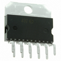
TDA7350 STMicroelectronics, TDA7350 Datasheet - Page 13

TDA7350
Manufacturer Part Number
TDA7350
Description
IC AMP AUDIO PWR 22W MULTIWATT11
Manufacturer
STMicroelectronics
Type
Class ABr
Datasheet
1.TDA7350.pdf
(22 pages)
Specifications of TDA7350
Output Type
1-Channel (Mono) or 2-Channel (Stereo)
Max Output Power X Channels @ Load
22W x 1 @ 3.2 Ohm; 11W x 2 @ 2 Ohm
Voltage - Supply
8 V ~ 18 V
Features
Depop, Short-Circuit and Thermal Protection, Standby
Mounting Type
Through Hole
Package / Case
Multiwatt-11 (Vertical, Bent and Staggered Leads)
Lead Free Status / RoHS Status
Lead free / RoHS Compliant
Available stocks
Company
Part Number
Manufacturer
Quantity
Price
Company:
Part Number:
TDA7350
Manufacturer:
FAI
Quantity:
2 189
Part Number:
TDA7350
Manufacturer:
CN/如韵
Quantity:
20 000
Figure 28: ICV - PNP Gain vs. I
Figure 29: ICV - PNP V
Figure 30: ICV - PNP cut-off frequency vs. I
CE(sat
) vs. I
C
C
C
OUTPUT STAGE
Poor current capability and low cutoff frequency
are well known limits of the standard lateral PNP.
Composite PNP-NPN power output stages have
been widely used, regardless their high saturation
drop. This drop can be overcome only at the ex-
pense of external components, namely, the boot-
strap capacitors. The availability of 4A isolated
collector PNP (ICV PNP) adds versatility to the
design. The performance of this component, in
terms of gain, V
shown in fig. 28, 29, 30 respectively. It is realized
in a new bipolar technology, characterized by top-
bottom isolation techniques, allowing the imple-
mentation of low leakage diodes, too. It guaran-
tees BV
NPN and PNP transistors. Basically, the connec-
tion shown in fig. 31 has been chosen. First of all
because its voltage swing is rail-to-rail, limited
only by the VCEsat of the output transistors,
which are in the range of 0.3
gain VOUT/VIN is greater than unity, approxi-
mately 1+R2/R1. (VCC/2 is fixed by an auxiliary
amplifier common to both channel). It is possible,
controlling the amount of this local feedback, to
force the loop gain (A . ) to less than unity at fre-
quencies for which the phase shift is 180°. This
means that the output buffer is intrinsically stable
and not prone to oscillation.
Figure 31: The New Output Stage
In contrast, with the circuit of fig. 32, the solution
adopted to reduce the gain at high frequencies is
the use of an external RC network.
AMPLIFIER BLOCK DIAGRAM
The block diagram of each voltage amplifier is
shown in fig. 33. Regardless of production
spread, the current in each final stage is kept low,
with enough margin on the minimum, below which
cross-over distortion would appear.
CEO
> 20V and BV
CEsat
and cut-off frequency, is
CBO
each. Then, the
> 50V both for
TDA7350
13/22


