MAX9715ETE+ Maxim Integrated Products, MAX9715ETE+ Datasheet - Page 6
MAX9715ETE+
Manufacturer Part Number
MAX9715ETE+
Description
IC AMP AUDIO PWR 2.8W D 16TQFN
Manufacturer
Maxim Integrated Products
Type
Class Dr
Datasheet
1.MAX9715ETE.pdf
(13 pages)
Specifications of MAX9715ETE+
Output Type
2-Channel (Stereo)
Max Output Power X Channels @ Load
2.8W x 2 @ 4 Ohm
Voltage - Supply
4.5 V ~ 5.5 V
Features
Depop, Short-Circuit and Thermal Protection, Shutdown
Mounting Type
Surface Mount
Package / Case
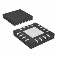
16-TQFN Exposed Pad
Product
Class-D
Output Power
2.8 W
Thd Plus Noise
0.06 %
Operating Supply Voltage
5 V
Supply Current
12.8 mA
Maximum Power Dissipation
1666 mW
Maximum Operating Temperature
+ 85 C
Mounting Style
SMD/SMT
Minimum Operating Temperature
- 40 C
Supply Voltage (max)
5.5 V
Supply Voltage (min)
4.5 V
Amplifier Class
D
No. Of Channels
2
Supply Voltage Range
4.5V To 5.5V
Load Impedance
4ohm
Operating Temperature Range
-40°C To +85°C
Amplifier Case Style
TQFN
Rohs Compliant
Yes
Lead Free Status / RoHS Status
Lead free / RoHS Compliant


2.8W, Low-EMI, Stereo, Filterless Class D
Audio Amplifier
(V
Typical Operating Circuit/Functional Diagram )
6
DD
_______________________________________________________________________________________
1, 12
PIN
4, 9
= 5.0V, C
10
11
13
14
15
16
—
2
3
5
6
7
8
0.40
0.35
0.30
0.25
0.20
0.15
0.10
0.05
0
VDD
4.5
OUTL+
OUTR+
OUTR-
NAME
OUTL-
PGND
SHDN
PV
GAIN
GND
BIAS
N.C.
V
INR
INL
EP
= 3 x 0.1μF, C
DD
DD
SHUTDOWN CURRENT
vs. SUPPLY VOLTAGE
4.8
SUPPLY VOLTAGE (V)
Power Ground
Left-Channel Positive Speaker Output
Left-Channel Negative Speaker Output
Positive Speaker Power-Supply Input. Power-supply input for speaker amplifier output stages. Connect
to V
No connection. Not internally connected.
Gain Select. Sets the internal amplifier gain. See the Gain Selection section.
Ground
Shutdown Control. Drive SHDN low to shut down the MAX9715.
Right-Channel Negative Speaker Output
Right-Channel Positive Speaker Output
Bias Voltage Output. V
Positive Power-Supply Input. Bypass to GND with a 0.1μF ceramic capacitor.
Right-Channel Input
Left-Channel Input
Exposed Paddle. Connect EP to an electrically isolated copper pad or GND.
5.0
DD
BIAS
and bypass with 0.1μF to PGND.
= 1μF, C
5.3
5.5
Typical Operating Characteristics (continued)
INL
BIAS
= C
= 1.8V, bypass BIAS to GND with a 1μF ceramic capacitor.
INR
= 1μF, A
V
= +10.5dB, T
FUNCTION
A
= +25°C, unless otherwise noted.) (See the
POWER-ON/OFF WAVEFORM
10ms/div
Pin Description
MAX9715 toc17
SHDN
5V/div
I
200mA/div
OUT
Related parts for MAX9715ETE+
Image
Part Number
Description
Manufacturer
Datasheet
Request
R

Part Number:
Description:
Filterless Class D Audio Amplifier
Manufacturer:
Maxim Integrated Products
Datasheet:

Part Number:
Description:
Max9715 2.8w, Low-emi, Stereo, Filterless Class D Audio Amplifier
Manufacturer:
Maxim Integrated Products, Inc.
Datasheet:
Part Number:
Description:
MAX7528KCWPMaxim Integrated Products [CMOS Dual 8-Bit Buffered Multiplying DACs]
Manufacturer:
Maxim Integrated Products
Datasheet:
Part Number:
Description:
Single +5V, fully integrated, 1.25Gbps laser diode driver.
Manufacturer:
Maxim Integrated Products
Datasheet:
Part Number:
Description:
Single +5V, fully integrated, 155Mbps laser diode driver.
Manufacturer:
Maxim Integrated Products
Datasheet:
Part Number:
Description:
VRD11/VRD10, K8 Rev F 2/3/4-Phase PWM Controllers with Integrated Dual MOSFET Drivers
Manufacturer:
Maxim Integrated Products
Datasheet:
Part Number:
Description:
Highly Integrated Level 2 SMBus Battery Chargers
Manufacturer:
Maxim Integrated Products
Datasheet:
Part Number:
Description:
Current Monitor and Accumulator with Integrated Sense Resistor; ; Temperature Range: -40°C to +85°C
Manufacturer:
Maxim Integrated Products
Part Number:
Description:
TSSOP 14/A°/RS-485 Transceivers with Integrated 100O/120O Termination Resis
Manufacturer:
Maxim Integrated Products
Part Number:
Description:
TSSOP 14/A°/RS-485 Transceivers with Integrated 100O/120O Termination Resis
Manufacturer:
Maxim Integrated Products
Part Number:
Description:
QFN 16/A°/AC-DC and DC-DC Peak-Current-Mode Converters with Integrated Step
Manufacturer:
Maxim Integrated Products
Part Number:
Description:
TDFN/A/65V, 1A, 600KHZ, SYNCHRONOUS STEP-DOWN REGULATOR WITH INTEGRATED SWI
Manufacturer:
Maxim Integrated Products
Part Number:
Description:
Integrated Temperature Controller f
Manufacturer:
Maxim Integrated Products
Part Number:
Description:
SOT23-6/I°/45MHz to 650MHz, Integrated IF VCOs with Differential Output
Manufacturer:
Maxim Integrated Products
Part Number:
Description:
SOT23-6/I°/45MHz to 650MHz, Integrated IF VCOs with Differential Output
Manufacturer:
Maxim Integrated Products