LM4666SD National Semiconductor, LM4666SD Datasheet - Page 3
LM4666SD
Manufacturer Part Number
LM4666SD
Description
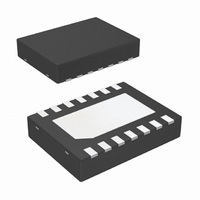
IC AMP AUDIO 1.2W STER D 14LLP
Manufacturer
National Semiconductor
Series
Boomer®r
Type
Class Dr
Datasheet
1.LM4666SD.pdf
(15 pages)
Specifications of LM4666SD
Output Type
2-Channel (Stereo)
Max Output Power X Channels @ Load
1.2W x 2 @ 8 Ohm
Voltage - Supply
2.8 V ~ 5.5 V
Features
Depop, Differential Inputs, Short-Circuit Protection, Shutdown
Mounting Type
Surface Mount
Package / Case
14-LLP
For Use With
LM4666SDBD - BOARD EVALUATION LM4666SD
Lead Free Status / RoHS Status
Lead free / RoHS Compliant
Other names
LM4666SD/NOPB
LM4666SDTR
LM4666SDTR
Available stocks
Company
Part Number
Manufacturer
Quantity
Price

Part Number:
LM4666SD
Manufacturer:
NS/国半
Quantity:
20 000
Company:
Part Number:
LM4666SD/NOPB
Manufacturer:
NS
Quantity:
525
Part Number:
LM4666SDX
Manufacturer:
NS/国半
Quantity:
20 000
Company:
Part Number:
LM4666SDX/NOPB
Manufacturer:
W
Quantity:
6 219


I
I
V
V
V
V
A
A
V
T
P
THD+N
X
R
PSRR
CMRR
SNR
e
DD
SD
Symbol
OUT
WU
SDIH
SDIL
GSIH
GSIL
V
V
OS
o
TALK
IN
Absolute Maximum Ratings
If Military/Aerospace specified devices are required,
please contact the National Semiconductor Sales Office/
Distributors for availability and specifications.
Electrical Characteristics V
The following specifications apply for V
25˚C.
Supply Voltage (Note1)
Storage Temperature
Voltage at Any Input Pin
Power Dissipation (Note 3)
ESD Susceptibility,
pins 4, 7, 11, 14 (Note 4)
ESD Susceptibility,
all other pins (Note 4)
ESD Susceptibility (Note 5)
Quiescent Power Supply Current
Shutdown Current
Shutdown Voltage Input High
Shutdown Voltage Input Low
Gain Select Input High
Gain Select Input Low
Closed Loop Gain
Closed Loop Gain
Output Offset Voltage
Wake-up Time
Output Power
Total Harmonic Distortion+Noise
Channel Separation
Differential Input Resistance
Power Supply Rejection Ratio
Common Mode Rejection Ratio
Signal to Noise Ratio
Output Noise
Parameter
V
DD
+ 0.3V ≥ V ≥ GND - 0.3V
DD
= 5V and R
Internally Limited
−65˚C to +150˚C
DD
V
V
V
V
V
THD = 1% (max), f = 1kHz,
22kHz BW
P
f
Both channels in phase
P
V
V
V
f
Inputs terminated to AC GND
V
f
P
V
f
P
A-Weighted filter, V
(Notes 1, 2)
IN
RIPPLE
RIPPLE
Ripple
IN
IN
SD
Gain Select
Gain Select
O
O
Gain Select
Gain Select
Ripple
Ripple
OUT
Ripple
O
= 1kHz, 22kHz BW,
= 5V
= 100mW
= 100mW
= 1W
= 0V, No Load
= 0V, R
= GND (Note 9)
= 10mW,1kHz
= 217Hz, Input referred
L
= 100mV
= 100mV
= 100mV
2.0kV
= 217Hz
= 217Hz
200V
6.0V
= 15µH + 8Ω + 15µH unless otherwise specified. Limits apply for T
RMS
1kV
= V
= GND
= V
= GND
L
Conditions
; A-Weighted Filter
(Notes 1, 2)
RMS
RMS
= 15µH + 8Ω + 15µH
DD
DD
3
RMS
RMS
RMS
/Channel,
, f = 1kHz
in
Operating Ratings
,
Junction Temperature (T
Thermal Resistance
Soldering Information
See AN-1112 "microSMD Wafers Level Chip Scale
Package."
Temperature Range
Supply Voltage
sine wave,
sine wave,
= 0V
θ
θ
T
JA
JC
MIN
(SDA)
(SDA)
≤ T
A
≤ T
MAX
(Note 6)
Typical
0.02
0.65
200
1.2
1.1
1.2
1.1
1.2
15
16
12
10
57
90
60
60
65
48
83
6
6
J
)
LM4666
(Notes 1, 2)
(Notes 7, 8)
Limit
−40˚C ≤ T
2.8V ≤ V
www.national.com
DD
(Limits)
A
Units
63˚C/W
12˚C/W
mA
mA
mV
≤ 85˚C
ms
kΩ
kΩ
µA
dB
dB
dB
dB
dB
dB
dB
µV
≤ 5.5V
W
%
150˚C
V
V
V
V
A
=
Related parts for LM4666SD
Image
Part Number
Description
Manufacturer
Datasheet
Request
R

Part Number:
Description:
National Semiconductor [8-Bit D/A Converter]
Manufacturer:
National Semiconductor
Datasheet:
Part Number:
Description:
National Semiconductor [Media Coprocessor]
Manufacturer:
National Semiconductor
Datasheet:
Part Number:
Description:
Digitally Controlled Tone and Volume Circuit with Stereo Audio Power Amplifier, Microphone Preamp Stage and National 3D Sound
Manufacturer:
National Semiconductor
Datasheet:
Part Number:
Description:
Digitally Controlled Tone and Volume Circuit with Stereo Audio Power Amplifier, Microphone Preamp Stage and National 3D Sound
Manufacturer:
National Semiconductor
Datasheet:
Part Number:
Description:
AC97 Rev 2 Codec with Sample Rate Conversion and National 3D Sound
Manufacturer:
National Semiconductor
Part Number:
Description:
Manufacturer:
National Semiconductor
Datasheet:
Part Number:
Description:
Manufacturer:
National Semiconductor
Datasheet:
Part Number:
Description:
General Purpose, Low Voltage, Low Power, Rail-to-Rail Output Operational Amplifiers
Manufacturer:
National Semiconductor
Datasheet:
Part Number:
Description:
8-bit 20 MSPS flash A/D converter.
Manufacturer:
National Semiconductor
Datasheet:
Part Number:
Description:
Low Noise Quad Operational Amplifier
Manufacturer:
National Semiconductor
Datasheet:
Part Number:
Description:
Quad Differential Line Receivers
Manufacturer:
National Semiconductor
Datasheet:
Part Number:
Description:
Quad High Speed Trapezoidal? Bus Transceiver
Manufacturer:
National Semiconductor
Datasheet:
Part Number:
Description:
Dual Line Receiver
Manufacturer:
National Semiconductor
Datasheet:
Part Number:
Description:
TTL to 10k ECL Level Translator with Latch
Manufacturer:
National Semiconductor
Datasheet: