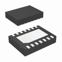
LM4666SD National Semiconductor, LM4666SD Datasheet

LM4666SD
Specifications of LM4666SD
LM4666SDTR
Available stocks
Related parts for LM4666SD
LM4666SD Summary of contents
Page 1
... The LM4666 has short circuit protection against a short from the outputs GND. DD Typical Application FIGURE 1. Typical Audio Amplifier Application Circuit Boomer ® registered trademark of National Semiconductor Corporation. © 2004 National Semiconductor Corporation Key Specifications j Efficiency at 3V, 100mW into 8Ω transducer 79% (typ) j Efficiency at 3V, 450mW into 8Ω transducer 84% (typ) j Efficiency at 5V, 1W into 8Ω ...
Page 2
... Connection Diagrams www.national.com SDA Package Top View Order Number LM4666SDA See NS Package Number SDA14A SDA Marking 200558I9 Top View Z — Plant Code XY — Date Code TT — Die Traceability L4666 — LM4666 2 200558I8 ...
Page 3
... Absolute Maximum Ratings If Military/Aerospace specified devices are required, please contact the National Semiconductor Sales Office/ Distributors for availability and specifications. Supply Voltage (Note1) Storage Temperature + 0.3V ≥ V ≥ GND - 0.3V Voltage at Any Input Pin V DD Power Dissipation (Note 3) ESD Susceptibility, pins 4, 7, 11, 14 (Note 4) ...
Page 4
Electrical Characteristics V The following specifications apply for V 25˚C. Symbol Parameter I Quiescent Power Supply Current DD I Shutdown Current SD V Shutdown Voltage Input High SDIH V Shutdown Voltage Input Low SDIL V Gain Select Input High GSIH ...
Page 5
External Components Description (Figure 1) Components 1. C Supply bypass capacitor which provides power supply filtering. Refer to the Power Supply Bypassing S section for information concerning proper placement and selection of the supply bypass capacitor Input AC ...
Page 6
Typical Performance Characteristics THD+N vs Output Power/Channel 15µH + 4Ω + 15µ 1kHz, 22kHz BW CMRR vs Frequency 15µH + 8Ω + 15µ ...
Page 7
Typical Performance Characteristics Efficiency and Power Dissipation vs Output Power = 15µH + 8Ω + 15µ 1kHz, THD ≤ 5V Efficiency and Power Dissipation vs Output Power = 15µH + 4Ω + ...
Page 8
Typical Performance Characteristics Output Power/Channel vs Supply Voltage R = 15µH + 8Ω + 15µ 1kHz L 22kHz BW Shutdown Threshold Shutdown Threshold vs Supply Voltage R = 15µH + 8Ω + 15µH L ...
Page 9
Typical Performance Characteristics Supply Current vs Supply Voltage R = 15µH + 8Ω + 15µH L (Note 10) (Continued) 20055824 9 www.national.com ...
Page 10
Application Information GENERAL AMPLIFIER FUNCTION The output signals generated by the LM4666 consist of two, BTL connected, output signals that pulse momentarily from near ground potential each channel. The two DD outputs on a given channel can ...
Page 11
Application Information typical value. Increased THD may also be observed with voltages less than V on the Shutdown pin when in PLAY DD mode. The LM4666 has an internal resistor connected between GND and Shutdown pins. The purpose of this ...
Page 12
Application Information CIRCUIT CONFIGURATIONS FIGURE 2. Single-Ended input with low gain selection configuration FIGURE 3. Differential input with low gain selection configuration www.national.com (Continued) 12 20055803 20055802 ...
Page 13
Application Information REFERENCE DESIGN BOARD SCHEMATIC In addition to the minimal parts required for the application circuit, a measurement filter is provided on the evaluation circuit board so that conventional audio measurements can be conveniently made without additional equipment. This ...
Page 14
Application Information LM4666 SDA BOARD ARTWORK Composite View Top Layer Internal Layer 2, V www.national.com (Continued) 20055805 20055809 DD 20055807 14 Silk Screen 20055808 Internal Layer 1, GND 20055806 Bottom Layer 20055804 ...
Page 15
... National does not assume any responsibility for use of any circuitry described, no circuit patent licenses are implied and National reserves the right at any time without notice to change said circuitry and specifications. inches (millimeters) unless otherwise noted LLP Package Order NumberLM4666SD NS Package Number SDA14A 2. A critical component is any component of a life ...


