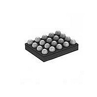
MAX97001EWP+T Maxim Integrated Products, MAX97001EWP+T Datasheet - Page 30

MAX97001EWP+T
Manufacturer Part Number
MAX97001EWP+T
Description
IC AUDIO SUBSYSTEM 20WLP
Manufacturer
Maxim Integrated Products
Series
DirectDrive™r
Type
Class Dr
Datasheet
1.MAX97001EWPT.pdf
(37 pages)
Specifications of MAX97001EWP+T
Output Type
1-Channel (Mono) with Stereo Headphones
Max Output Power X Channels @ Load
920mW x 1 @ 8 Ohm; 37mW x 2 @ 16 Ohm
Voltage - Supply
2.7 V ~ 5.5 V
Features
Depop, Differential Inputs, I²C, Mute, Shutdown, Volume Control
Mounting Type
Surface Mount
Package / Case
20-WLP
Product
Class-D
Output Power
550 mW, 700 mW, 920 mW
Available Set Gain
12 dB
Common Mode Rejection Ratio (min)
32 dB, 55 dB
Thd Plus Noise
0.05 %
Operating Supply Voltage
2.7 V to 5.5 V
Supply Current
2.7 V
Maximum Power Dissipation
1040 mW
Maximum Operating Temperature
+ 85 C
Mounting Style
SMD/SMT
Input Signal Type
Differential, Single
Minimum Operating Temperature
- 40 C
Output Signal Type
Differential
Supply Voltage (max)
5.5 V
Lead Free Status / RoHS Status
Lead free / RoHS Compliant
Other names
MAX97001EWP+T
Audio Subsystem with Mono Class D Speaker
and Class H Headphone Amplifiers
Table 7. Charge-Pump Control Register
The MAX97001 features an I
2-wire serial interface consisting of a serial-data line
(SDA) and a serial-clock line (SCL). SDA and SCL facili-
tate communication between the MAX97001 and the
master at clock rates up to 400kHz. Figure 1 shows the
2-wire interface timing diagram. The master generates
SCL and initiates data transfer on the bus. The master
device writes data to the MAX97001 by transmitting the
proper slave address followed by the register address
and then the data word. Each transmit sequence is
framed by a START or REPEATED START (Sr) condi-
tion and a STOP (P) condition. Each word transmitted
to the MAX97001 is 8 bits long and is followed by an
acknowledge clock pulse. A master reading data from
the MAX97001 transmits the proper slave address fol-
lowed by a series of nine SCL pulses. The MAX97001
transmits data on SDA in sync with the master-generated
SCL pulses. The master acknowledges receipt of each
byte of data. Each read sequence is framed by a START
or REPEATED START condition, a not acknowledge,
and a STOP condition. SDA operates as both an input
and an open-drain output. A pullup resistor, typically
greater than 500I, is required on SDA. SCL operates
only as an input. A pullup resistor, typically greater than
500I, is required on SCL if there are multiple masters
on the bus, or if the single master has an open-drain
SCL output. Series resistors in line with SDA and SCL
are optional. Series resistors protect the digital inputs
of the MAX97001 from high-voltage spikes on the bus
lines and minimize crosstalk and undershoot of the bus
signals.
SMBus is a trademark of Intel Corp.
30
REGISTER
0x09
BIT
1
0
CPSEL
NAME
FIXED
2
I
C/SMBusK-compatible,
2
C Serial Interface
Charge-Pump Output Select. Works with the FIXED to set Q1.8V or Q0.9V outputs on
HPVDD and HPVSS. Ignored when FIXED = 0.
0 = Q1.8V on HPVDD/HPVSS
1 = Q0.9V on HPVDD/HPVSS
Class H Mode. When enabled, this bit forces the charge pump to generate static power
rails for HPVDD and HPVSS, instead of dynamically adjusting them based on output
signal level.
0 = Class H mode
1 = Fixed-supply mode
Figure 8. START, STOP, and REPEATED START Conditions
One data bit is transferred during each SCL cycle. The data
on SDA must remain stable during the high period of the
SCL pulse. Changes in SDA while SCL is high are control
signals (see the START and STOP Conditions section).
SDA and SCL idle high when the bus is not in use. A
master initiates communication by issuing a START con-
dition. A START condition is a high-to-low transition on
SDA with SCL high. A STOP condition is a low-to-high
transition on SDA while SCL is high (Figure 8). A START
condition from the master signals the beginning of a
transmission to the MAX97001. The master terminates
transmission, and frees the bus, by issuing a STOP con-
dition. The bus remains active if a REPEATED START
condition is generated instead of a STOP condition.
SDA
SCL
DESCRIPTION
S
START and STOP Conditions
Charge-Pump Control
Sr
Bit Transfer
P


