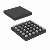
LM49350RL/NOPB National Semiconductor, LM49350RL/NOPB Datasheet - Page 34

LM49350RL/NOPB
Manufacturer Part Number
LM49350RL/NOPB
Description
IC AUDIO SUBSYSTM 2W D 36USMDXT
Manufacturer
National Semiconductor
Series
Boomer®r
Type
Class Dr
Datasheet
1.LM49350RLNOPB.pdf
(104 pages)
Specifications of LM49350RL/NOPB
Output Type
1-Channel (Mono) with Mono and Stereo Headphones
Max Output Power X Channels @ Load
2W x 1 @ 4 Ohm; 69mW x 2 @ 32 Ohm
Voltage - Supply
2.7 V ~ 5.5 V
Features
3D, DAC, Depop, I²C, I²S, Mute, Short-Circuit and Thermal Protection, Shutdown, Volume Control
Mounting Type
Surface Mount
Package / Case
36-MicroSMDxt
Lead Free Status / RoHS Status
Lead free / RoHS Compliant
Other names
LM49350RLTR
www.national.com
18.0 LM49350 Clock Network
(Refer to Figure 12)
The audio DAC and ADC operate at a clock frequency of
2*OSR*f
sampling frequency of the DAC or ADC. The DAC can operate
at four different OSR settings (128, 125, 64, 32). The ADC
can operate at three different OSR settings (128, 125, 64).
For example, if the stereo DAC or ADC is set at OSR = 128,
a 12.288MHz clock is required for 48kHz data. If a 12.288MHz
clock is not available, then one of the LM49350's dual PLLs
can be used to generate the desired clock frequency. Other-
wise, if a 12.288MHz is available, then the PLL can be by-
passed to reduce power consumption. The DAC clock divider
(S divider) or ADC clock divider (T divider) can also be used
to generate the correct clock. If an 18.432 MHz clock is avail-
able, the S or T divider could be set to 1.5 in order to generate
a 12.288MHz clock from 18.432MHz without using a PLL.
DAC Sample Rate
ADC Sample Rate
11.025
S
(kHz)
22.05
44.1
192
where OSR is the oversampling ratio and f
12
16
24
32
48
96
8
11.025
22.05
(kHz)
44.1
12
16
24
32
48
8
Clock Required at A
11.2896 MHz
(OSR = 128)
2.8224 MHz
5.6448 MHz
12.288 MHz
24.576 MHz
2.048 MHz
3.072 MHz
4.096 MHz
6.144 MHz
8.192 MHz
Clock Required at B
—
11.2896 MHz
(OSR = 128)
2.8224 MHz
5.6448 MHz
12.288 MHz
2.048 MHz
3.072 MHz
4.096 MHz
6.144 MHz
8.192 MHz
TABLE 5. DAC Clock Requirements
TABLE 6. ADC Clock Requirements
Clock Required at A
S
is the
2.75625 MHz
(OSR= 125)
5.5125 MHz
11.025 MHz
12 MHz
24 MHz
2 MHz
3 MHz
4 MHz
6 MHz
8 MHz
—
34
The DAC path clock (DAC_SOURCE_CLK) and ADC path
clock (ADC_SOURCE_CLK) can be driven directly by the
MCLK input, the PORT1_CLK input, the PORT2_CLK input,
PLL1's output, or PLL2's output.
For instances where a PLL must be used, the PLL input clock
can come from three sources. The clock input to PLL1 or PLL2
can come from the MCLK input, the PORT1_CLK input, or the
PORT2_CLK input.
The LM49350's Power Management Circuit (PMC) requires
a clock that is independent from the DAC or ADC. It is rec-
ommended to provide a
clock divider (R divider) is available to generate the correct
clock to the PMC block. The PMC clock path can be driven
directly by the MCLK input, the internal 300kHz oscillator, the
DAC_SOURCE_CLK, or the ADC_SOURCE_CLK.
Clock Required at B
2.75625 MHz
5.5125 MHz
11.025 MHz
(OSR= 125)
12 MHz
2 MHz
3 MHz
4 MHz
6 MHz
8 MHz
Clock Required at A
1.4112 MHz
2.8224 MHz
5.6448 MHz
12.288 MHz
24.576 MHz
(OSR = 64)
1.024 MHz
1.536 MHz
2.048 MHz
3.072 MHz
4.096 MHz
6.144 MHz
≈
300kHz clock at Point C. The PMC
Clock Required at B
Clock Required at A
1.4112 MHz
2.8224 MHz
5.6448 MHz
(OSR = 64)
1.024 MHz
1.536 MHz
2.048 MHz
3.072 MHz
4.096 MHz
6.144 MHz
0.7056 MHz
1.4112 MHz
2.8224 MHz
12.288 MHz
(OSR = 32)
0.512 MHz
0.768 MHz
1.024 MHz
1.536 MHz
3.072 MHz
6.144 MHz
2.048MHz


