LM4937RL/NOPB National Semiconductor, LM4937RL/NOPB Datasheet - Page 34
LM4937RL/NOPB
Manufacturer Part Number
LM4937RL/NOPB
Description
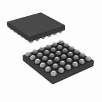
IC AUDIO SUBSYSTM 1.25W 36USMDXT
Manufacturer
National Semiconductor
Series
Boomer®r
Type
Class ABr
Datasheet
1.LM4937TLNOPB.pdf
(42 pages)
Specifications of LM4937RL/NOPB
Output Type
1-Channel (Mono) with Mono and Stereo Headphones
Max Output Power X Channels @ Load
1.25W x 1 @ 8 Ohm; 80mW x 2 @ 32 Ohm
Voltage - Supply
2.7 V ~ 5.5 V
Features
Depop, Differential Inputs, I²C, I²S, Mute, Shutdown, SPI, Volume Control
Mounting Type
Surface Mount
Package / Case
36-MicroSMDxt
Lead Free Status / RoHS Status
Lead free / RoHS Compliant
Other names
LM4937RLTR


www.national.com
Application Information
I
The LM4937 supports both master and slave I2S transmis-
sion at either 16 or 32 bits per word at clock rates up to
MONO ONLY SETTING
The LM4937 may be restricted to mono amplification only by
setting D-6 in Output Control register 0x01h to 1. This may
save an additional 400μA from I
LM4937 DEMOBOARD OPERATION
BOARD LAYOUT
DIGITAL SUPPLIES
JP14 — Digital Power DVDD
JP10 — I/O Power IOVDD
JP13 — PLL Supply PLLVDD
JP16 — USB Board Supply BBVDD
JP15 — I2C VDD
All supplies may be set independently. All digital ground is
common. Jumpers may be used to connect all the digital sup-
plies together.
S9 – connects VDD_PLL to VDD_D
S10 – connects VDD_D to VDD_IO
S11 – connects VDD_IO to VDD_I2C
S12 – connects VDD_I2C to Analog VDD
S17 – connects BB_VDD to USB3.3V (from USB board)
S19 – connects VDD_D to USB3.3V (from USB board)
S20 – connects VDD_D to SPDIF receiver chip
ANALOG SUPPLY
JP11 — Analog Supply
INPUTS
Analog Inputs
JP2 — Mono Differential Input
JP6 — Left Input
JP7 — Right Input
Digital Inputs
JP19 — Digital Interface
2
S12 — connects Analog VDD with Digital VDD (I2C_VDD)
S16 — connects Analog Ground with Digital Ground
S21 — connects Analog VDD to SPDIF receiver chip
Pin 1 — MCLK
Pin 2 — I2S_CLK
Pin 3 — I2S_SDI
S
DD
.
FIGURE 4.
34
3.072MHz (48kHz stereo, 32bit). The basic format is shown
below:
JP20 — Toslink SPDIF Input
JP21 — Coaxial SPDIF Input
Coaxial and Toslink inputs may be toggled between by use of
S25. Only one may be used at a time. Must be used in con-
junction with on-board SPDIF receiver chip.
OUTPUTS
JP5 — BTL Loudspeaker Output
JP1 — Left Headphone Output (Single-Ended or OCL)
JP3 — Right Headphone Output (Single-Ended or OCL)
P1 — Stereo Headphone Jack (Same as JP1, JP2, Single-
Ended or OCL)
JP12 — Mono BTL Earpiece Output
CONTROL INTERFACE
X1, X2 – USB Control Bus for I2C/SPI
X1
Pin 9 – Mode Select (SPI or I2C)
X2
Pin 1 – SDA
Pin 3 – SCL
Pin 15 – ADDR/END
Pin 14 – USB5V
Pin 16 – USB3.3V
Pin 16 – USB GND
MISCELLANEOUS
I2S BUS SELECT
S23, S24, S26, S27 – I2S Bus select. Toggles between on-
board and external I2S (whether on-board SPDIF receiver is
used). All jumpers must be set the same. Jumpers on top two
pins selects external bus (JP19). Jumpers on bottom two pins
selects on-board SPDIF receiver output.
HEADPHONE OUTPUT CONFIGURATION
Jumpers S1, S2, S3, and S4 are used to configure the head-
phone outputs for either cap-coupled outputs or output ca-
pacitorless (OCL) mode in addition to the register control
internal to the LM4937 for this feature. Jumpers S1 and S3
bypass the output DC blocking capacitors when OCL mode
Pin 4 — I2S_WS
20202007
Related parts for LM4937RL/NOPB
Image
Part Number
Description
Manufacturer
Datasheet
Request
R

Part Number:
Description:
Manufacturer:
National Semiconductor
Datasheet:
Part Number:
Description:
National Semiconductor [8-Bit D/A Converter]
Manufacturer:
National Semiconductor
Datasheet:
Part Number:
Description:
National Semiconductor [Media Coprocessor]
Manufacturer:
National Semiconductor
Datasheet:
Part Number:
Description:
Digitally Controlled Tone and Volume Circuit with Stereo Audio Power Amplifier, Microphone Preamp Stage and National 3D Sound
Manufacturer:
National Semiconductor
Datasheet:
Part Number:
Description:
Digitally Controlled Tone and Volume Circuit with Stereo Audio Power Amplifier, Microphone Preamp Stage and National 3D Sound
Manufacturer:
National Semiconductor
Datasheet:
Part Number:
Description:
AC97 Rev 2 Codec with Sample Rate Conversion and National 3D Sound
Manufacturer:
National Semiconductor
Part Number:
Description:
Manufacturer:
National Semiconductor
Datasheet:
Part Number:
Description:
Manufacturer:
National Semiconductor
Datasheet:
Part Number:
Description:
General Purpose, Low Voltage, Low Power, Rail-to-Rail Output Operational Amplifiers
Manufacturer:
National Semiconductor
Datasheet:
Part Number:
Description:
8-bit 20 MSPS flash A/D converter.
Manufacturer:
National Semiconductor
Datasheet:
Part Number:
Description:
Low Noise Quad Operational Amplifier
Manufacturer:
National Semiconductor
Datasheet:
Part Number:
Description:
Quad Differential Line Receivers
Manufacturer:
National Semiconductor
Datasheet:
Part Number:
Description:
Quad High Speed Trapezoidal? Bus Transceiver
Manufacturer:
National Semiconductor
Datasheet:
Part Number:
Description:
Dual Line Receiver
Manufacturer:
National Semiconductor
Datasheet: