LM4937RL/NOPB National Semiconductor, LM4937RL/NOPB Datasheet
LM4937RL/NOPB
Specifications of LM4937RL/NOPB


Related parts for LM4937RL/NOPB

LM4937RL/NOPB Summary of contents
Page 1
... The full range music path features an SNR of 85dB with a 192kHz playback. Boomer audio power amplifiers are designed specifically to provide high quality output power with a minimal amount of external components. Boomer® registered trademark of National Semiconductor Corporation. © 2007 National Semiconductor Corporation Key Specifications ■ P OUT ■ ...
Page 2
Block Diagram FIGURE 1. Audio Sub-System Block Diagram with OCL HP Outputs www.national.com (HP outputs may also be configured as cap-coupled) 2 20202001 ...
Page 3
Connection Diagrams 36 – Bump Micro SMD Top View (Bump Side Down) Order Number LM4937TL See NS Package Number TLA36LVA 36 – Bump Micro SMD Top View (Bump Side Down) Order Number LM4937RL See NS Package Number RLA36LVA 36 – ...
Page 4
Pin Descriptions Pin Pin Name Digital/ Analog A1 DGND D A2 MCLK D A3 I2S_WS D A4 SDA/SDI D A5 DVDD D A6 VDD_IO D B1 PLL_VDD D B2 I2S_SDATA D B3 I2S_CLK D B4 GPIO D B5 I2C_VDD D ...
Page 5
... Absolute Maximum Ratings If Military/Aerospace specified devices are required, please contact the National Semiconductor Sales Office/ Distributors for availability and specifications. Analog Supply Voltage Digital Supply Voltage Storage Temperature Input Voltage Power Dissipation (Note 3) ESD Susceptibility (Note 4) ESD Susceptibility (Note 5) Junction Temperature ...
Page 6
Audio Amplifier Electrical Characteristics AV The following specifications apply for the circuit shown in Figure 1 with all programmable gain set at 0dB, unless otherwise specified. Limits apply for T = 25°C. A Symbol Parameter I Supply Current DD I ...
Page 7
Volume Control Electrical Characteristics The following specifications apply for 3. 25°C. A Symbol Parameter Stereo Analog Inputs PreAmp Gain Setting Range PGR Differential Mono Analog Input PreAmp Gain Setting Range Output Volume Control for VCR Loudspeaker, Headphone Output, ...
Page 8
Symbol Parameter ≤ ≤ SPI (1. 2.2V Maximum SPI Frequency SPI t SPI Data Setup Time SPISETD t SPI ENB Setup Time SPISETENB t SPI Data Hold Time SPIHOLDD t SPI ENB Hold ...
Page 9
Symbol Parameter V Digital Input High Voltage IH V Digital Input Low Voltage IL Note 1: All voltages are measured with respect to the GND pin unless otherwise specified. Note 2: Absolute Maximum Ratings indicate limits beyond which damage to ...
Page 10
Output Noise AV = 5.0V and AV DD MODE PSRR AV = 3.0V 217Hz ripple MODE EP(Typ ...
Page 11
System Control The LM4937 is controlled via either a two wire I This interface is used to configure the operating mode, interfaces, data converters, mixers and amplifiers. The LM4937 is controlled by writing 8 bit data into a series of ...
Page 12
When the part is configured ADDR is low then the address portion of the I address input should be set to write to 1110000 Chip Address 0 EC ADR = ...
Page 13
13 www.national.com ...
Page 14
www.national.com 14 ...
Page 15
System Controls TABLE 7. Loudspeaker, Earpiece, HP Left or Right Volume Control EP_VOL_4, EP_VOL_3, LS_VOL_4, LS_VOL_3, HP_L_VOL_4, HP_L_VOL_3, HP_R_VOL_4 HP_R_VOL_3 ...
Page 16
Mode CD3 CD2 — Shutdown M — Mono Differential Input AL — Analog Left Channel ...
Page 17
Loudspeaker Headphone Left Channel Headphone Right Channel Earpiece All Outputs TABLE 10. Mono Differential Amplifier Input Gain Select (08h) MONO_IN_GAIN_2 MONO_IN_GAIN_1 TABLE 11. Analog Single-Ended Input Amplifier Gain Select (07h) ANA_L_GAIN_2 ANA_L_GAIN_1 ...
Page 18
PLL Configuration Registers PLL M DIVIDER CONFIGURATION REGISTER This register is used to control the input divider of the PLL. PLL_M (0Ah) (Set = logic 1, Clear = logic 0) Bits Register 6:0 PLL_M NOTES: The M divider should be ...
Page 19
PLL_P (0Dh) (Set = logic 1, Clear = logic 0) Bits Register 3:0 PLL_P NOTES: The output of this divider should be either 12 or 24MHz in USB mode or 11.2896MHz, 12.288MHz or 24.576MHz in non-USB modes. The division of ...
Page 20
Further Notes on PLL Programming The sigma-delta PLL is designed to drive audio circuits requiring accurate clock frequencies 25MHz with frequency errors noise-shaped away from the audio band. The 5 bits of modulus control provide exact synchronization ...
Page 21
If the user needs to obtain a clock unrelated to those described above, the following method is advised. An example of obtaining 11.2896 from 12.000MHz is shown below. Choose a small range that the VCO frequency is ...
Page 22
Bits Register 7:4 R_DIV By default the stereo DAC operates at 250*fs, i.e. 12.000MHz (at the clock generator input clock) for 48kHz data expected that the PLL be used to drive the audio system unless a 12.000MHz master ...
Page 23
Common Clock Settings for the DAC The DAC can work in 4 modes, each with different oversampling rates, 125,128,64 & 32. In normal operation 125x oversampling provides for the simplest clocking solution as it will work from 12.000MHz (common in ...
Page 24
R_DIV Divide Value DAC Clock Generator Input Frequency <MHz> 1 The R divider can also be used along with the P divider in order to create the clock needed to support low sample rates. www.national.com ...
Page 25
DAC Setup Register This register is used to configure the basic operation of the stereo DAC. DAC_SETUP (0Eh) (Set = logic 1, Clear = logic 0) Bits Register 1:0 DAC_MODE 2 MUTE_L 3 MUTE_R 4 DITHER_OFF 5 DITHER ALWAYS_ON ...
Page 26
Interface Control Register This register is used to control the I2S and I INTERFACE (0Fh) (Set = logic 1, Clear = logic 0) Bits NOTES: The master I2S format depends on the DAC mode. In USB ...
Page 27
FIR Compensation Filter Configuration Registers These registers are used to configure the DAC’s FIR com- pensation filter. Three 16 bit coefficients are required and → COMP_COEFF (10h 15h) (Set = logic 1, Clear = logic 0) Address Register 10h COMP_COEFF0_LSB ...
Page 28
Typical Performance Characteristics THD+N vs Frequency = 32Ω, P 3.0V EP Out THD+N vs Frequency = 8Ω, P 3.0V LS Out THD+N vs Frequency = 16Ω, P 5.0V HP Out www.national.com = 20mW O ...
Page 29
THD+N vs Frequency = 8Ω, P 5.0V LS Out 500mW L O 20202071 THD+N vs Output Power = 32Ω 1kHz 3.0V EP Out 20202073 THD+N vs Output Power = 32Ω 1kHz 3.0V ...
Page 30
THD+N vs Output Power = 16Ω 1kHz 5.0V EP Out THD+N vs Output Power = 16Ω 1kHz 5.0V HP Out THD+N vs Output Power = 8Ω 1kHz 5.0V LS Out, ...
Page 31
THD+N vs I2S Level HP Out 20202084 PSRR vs Frequency 3.0V EP Out Mode 1 20202086 PSRR vs Frequency 3.0V HP Out Mode 2 20202088 THD+N vs I2S Level LS Out PSRR vs Frequency 3.0V EP Out Mode 4 PSRR ...
Page 32
PSRR vs Frequency 3.0V LS Out Mode 2 PSRR vs Frequency 5.0V HP Out Mode 2 PSRR vs Frequency 5.0V LS Out Mode 4 www.national.com PSRR vs Frequency 3.0V LS Out Mode 4 20202090 PSRR vs Frequency 5.0V HP Out ...
Page 33
Output Power vs Supply Voltage = 32Ω, 1% THD+N EP Out , R L 20202096 Output Power vs Supply Voltage = 8Ω, 1% THD+N LS Out , R L 20202098 Output Power vs Supply Voltage = 32Ω, 1% THD+N HP ...
Page 34
Application Information The LM4937 supports both master and slave I2S transmis- sion at either bits per word at clock rates up to MONO ONLY SETTING The LM4937 may be restricted to mono amplification only ...
Page 35
S2 connects the center amplifer HPCOUT to the headphone ring when in OCL mode. S4 connects the center ring to GND when cap-coupled mode is desired. S4 must be removed for OCL mode to function properly. Jumper settings ...
Page 36
Demonstration Board Schematic www.national.com 36 ...
Page 37
37 www.national.com ...
Page 38
www.national.com 38 ...
Page 39
Revision History Rev 1.0 1.1 1.2 1.3 1.4 1.5 1.6 1.7 1.8 Date 10/04/06 Initial release. 10/13/06 Text edits. 12/15/06 Changed the datasheet title from RF Resistant Topology to RF Suppression. 02/09/07 Replaced curve (THD+N vs Output Power ...
Page 40
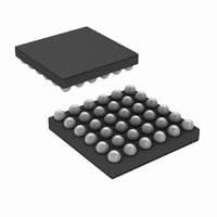
Physical Dimensions www.national.com inches (millimeters) unless otherwise noted 36-Bump micro SMD Order Number LM4937TL NS Package Number TLA36LVA = 3255±30μm, = 3510±30μ 600±75μ ...
Page 41
SMD Order Number LM4937RL NS Package Number RLA36LVA = 3255±30μm, = 3510±30μ 600±75μ www.national.com ...
Page 42
... For more National Semiconductor product information and proven design tools, visit the following Web sites at: Products Amplifiers www.national.com/amplifiers Audio www.national.com/audio Clock Conditioners www.national.com/timing Data Converters www.national.com/adc Displays www.national.com/displays Ethernet www.national.com/ethernet Interface www.national.com/interface LVDS www.national.com/lvds Power Management www.national.com/power Switching Regulators www.national.com/switchers LDOs www ...