LM4985TM/NOPB National Semiconductor, LM4985TM/NOPB Datasheet - Page 9
LM4985TM/NOPB
Manufacturer Part Number
LM4985TM/NOPB
Description
IC AMP AUDIO PWR .135W AB 12USMD
Manufacturer
National Semiconductor
Series
Boomer®r
Type
Class ABr
Datasheet
1.LM4985TMNOPB.pdf
(29 pages)
Specifications of LM4985TM/NOPB
Output Type
Headphones, 2-Channel (Stereo)
Max Output Power X Channels @ Load
135mW x 2 @ 16 Ohm
Voltage - Supply
2.3 V ~ 5.5 V
Features
I²C, Shutdown, Thermal Protection, Volume Control
Mounting Type
Surface Mount
Package / Case
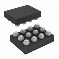
12-MicroSMD
Operational Class
Class-AB
Audio Amplifier Output Configuration
2-Channel Stereo
Output Power (typ)
135x2@16OhmW
Audio Amplifier Function
Headphone
Single Supply Voltage (typ)
3/5V
Dual Supply Voltage (typ)
Not RequiredV
Power Supply Requirement
Single
Rail/rail I/o Type
No
Power Supply Rejection Ratio
77dB
Single Supply Voltage (min)
2.3V
Single Supply Voltage (max)
5.5V
Dual Supply Voltage (min)
Not RequiredV
Dual Supply Voltage (max)
Not RequiredV
Operating Temp Range
-40C to 85C
Operating Temperature Classification
Industrial
Mounting
Surface Mount
Pin Count
12
For Use With
LM4985TMEVAL - BOARD EVALUATION LM4985TM
Lead Free Status / RoHS Status
Lead free / RoHS Compliant
Other names
LM4985TMTR


A
∆A
V
VMAX
OS
Electrical Characteristics V
The following specifications apply for R
25˚C.
Note 1: All voltages are measured with respect to the GND pin unless otherwise specified.
Note 2: Absolute Maximum Ratings indicate limits beyond which damage to the device may occur. Operating Ratings indicate conditions for which the device is
functional but do not guarantee specific performance limits. Electrical Characteristics state DC and AC electrical specifications under particular test conditions which
guarantee specific performance limits. This assumes that the device is within the Operating Ratings. Specifications are not guaranteed for parameters where no limit
is given, however, the typical value is a good indication of device performance.
Note 3: The maximum power dissipation must be derated at elevated temperatures and is dictated by TJMAX, θ
allowable power dissipation is P
currents for more information.
Note 4: Human Body Model: 100pF discharged through a 1.5kΩ resistor.
Note 5: Machine Model: 200pF ≤ C
Note 6: Typicals are measured at 25˚C and represent the parametric norm.
Note 7: Limits are guaranteed to National’s AOQL (Average Outgoing Quality Level).
Note 8: Datasheet min/max specification limits are guaranteed by design, test, or statistical analysis.
Note 9: 10Ω terminated input.
Note 10: The LDA10A package has its exposed-DAP soldered to an exposed 1.2in
Note 11: The wake-up time (T
External Components Description
Components
V
1.
2.
3.
6.
Symbol
C
C
C
C
S
B
o
I
Maximum Gain
Gain Accuracy per Step
Output Offset Voltage
Input coupling capacitor which blocks the DC voltage at the amplifier’s input terminals. Also creates a
high-pass filter with R
an explanation of how to determine the value of C
Supply bypass capacitor which provides power supply filtering. Refer to the Power Supply Bypassing
section for information concerning proper placement and selection of the supply bypass capacitor.
Bypass pin capacitor which provides half-supply filtering. Refer to the section, Proper Selection of Proper
Components, for information concerning proper placement and selection of C
Output coupling capacitor which blocks the DC voltage at the amplifier’s output. Forms a high pass filter with
R
L
at f
WU
DMAX
o
= 1/(2πR
) is calculated using the following formula; T
mm
Parameter
= (T
≤ 220pF discharged through all pins.
JMAX
L
C
- T
o
A
)
L
)/ θ
i
= 16Ω, f = 1kHz, and C
at f
JA
or the number given in Absolute Maximum Ratings, whichever is lower. For the LM4985, see power derating
c
DD
= 1/(2πR
= 2.5V
Code = 11111
18dB ≥ A
–44dB ≥ A
OCL
R
V
IN
LOAD
i
C
= AC GND
i
). Refer to the section Proper Selection of External Components, for
(Figure 2)
= 32Ω
Functional Description
WU
(Notes 1, 2) (Continued)
V
9
V
≥ –44dB
= [C
B
>
2
Conditions
= 4.7µF unless otherwise specified. Limits apply to T
area of 1oz. Printed circuit board copper.
–76dB
BYPASS
i
.
(VDD) / 2 (I
BYPASS
JA
, and the ambient temperature, T
)] + 40ms.
(Note 6)
±
±
B
Typ
2.0
18
0.5
1.0
LM4985
(Notes 7,
Limit
8)
A
. The maximum
www.national.com
(Limits)
A
Units
=
mV
dB
dB
Related parts for LM4985TM/NOPB
Image
Part Number
Description
Manufacturer
Datasheet
Request
R

Part Number:
Description:
National Semiconductor [8-Bit D/A Converter]
Manufacturer:
National Semiconductor
Datasheet:
Part Number:
Description:
National Semiconductor [Media Coprocessor]
Manufacturer:
National Semiconductor
Datasheet:
Part Number:
Description:
Digitally Controlled Tone and Volume Circuit with Stereo Audio Power Amplifier, Microphone Preamp Stage and National 3D Sound
Manufacturer:
National Semiconductor
Datasheet:
Part Number:
Description:
Digitally Controlled Tone and Volume Circuit with Stereo Audio Power Amplifier, Microphone Preamp Stage and National 3D Sound
Manufacturer:
National Semiconductor
Datasheet:
Part Number:
Description:
AC97 Rev 2 Codec with Sample Rate Conversion and National 3D Sound
Manufacturer:
National Semiconductor
Part Number:
Description:
Manufacturer:
National Semiconductor
Datasheet:
Part Number:
Description:
Manufacturer:
National Semiconductor
Datasheet:
Part Number:
Description:
General Purpose, Low Voltage, Low Power, Rail-to-Rail Output Operational Amplifiers
Manufacturer:
National Semiconductor
Datasheet:
Part Number:
Description:
8-bit 20 MSPS flash A/D converter.
Manufacturer:
National Semiconductor
Datasheet:
Part Number:
Description:
Low Noise Quad Operational Amplifier
Manufacturer:
National Semiconductor
Datasheet:
Part Number:
Description:
Quad Differential Line Receivers
Manufacturer:
National Semiconductor
Datasheet:
Part Number:
Description:
Quad High Speed Trapezoidal? Bus Transceiver
Manufacturer:
National Semiconductor
Datasheet:
Part Number:
Description:
Dual Line Receiver
Manufacturer:
National Semiconductor
Datasheet:
Part Number:
Description:
TTL to 10k ECL Level Translator with Latch
Manufacturer:
National Semiconductor
Datasheet: