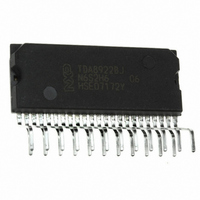
TDA8920CJ/N1,112 NXP Semiconductors, TDA8920CJ/N1,112 Datasheet - Page 17

TDA8920CJ/N1,112
Manufacturer Part Number
TDA8920CJ/N1,112
Description
IC AMP AUDIO PWR 220W 23SIL
Manufacturer
NXP Semiconductors
Type
Class Dr
Datasheet
1.TDA8920CJN1112.pdf
(39 pages)
Specifications of TDA8920CJ/N1,112
Output Type
1-Channel (Mono) or 2-Channel (Stereo)
Package / Case
23-SIL (Bent and Staggered Leads)
Max Output Power X Channels @ Load
220W x 1 @ 8 Ohm; 125W x 2 @ 4 Ohm
Voltage - Supply
±12.5 V ~ 32.5 V
Features
Depop, Differential Inputs, Mute, Short-Circuit and Thermal Protection, Standby
Mounting Type
Through Hole
Product
Class-D
Output Power
210 W
Available Set Gain
36 dB
Common Mode Rejection Ratio (min)
75 dB
Thd Plus Noise
0.05 %
Maximum Operating Temperature
+ 85 C
Mounting Style
Through Hole
Audio Load Resistance
8 Ohms
Dual Supply Voltage
+/- 30 V
Input Signal Type
Differential
Minimum Operating Temperature
- 40 C
Output Signal Type
Differential, Single
Supply Type
Dual
Lead Free Status / RoHS Status
Lead free / RoHS Compliant
Other names
568-4784-5
935281808112
TDA8920CJ/N1
TDA8920CJ/N1,112
TDA8920CJ/N1
935281808112
TDA8920CJ/N1
TDA8920CJ/N1,112
TDA8920CJ/N1
NXP Semiconductors
13. Application information
TDA8920C_2
Product data sheet
13.3.1 Single-Ended (SE)
13.1 Mono BTL application
13.2 Pin MODE
13.3 Estimating the output power
When using the power amplifier in a mono BTL application, the inputs of the two channels
must be connected in parallel and the phase of one of the inputs must be inverted; see
Figure
single-ended demodulation filters.
To ensure a pop noise-free start-up, an RC time-constant must be applied to pin MODE.
The bias-current setting of the VI converter input is directly related to the voltage on pin
MODE. In turn the bias-current setting of the VI converters is directly related to the DC
output offset voltage. A slow dV/dt on pin MODE results in a slow dV/dt for the DC output
offset voltage, ensuring a pop noise-free transition between Mute and Operating modes. A
time-constant of 500 ms is sufficient to guarantee pop noise-free start-up; see
Figure 5
Maximum output power:
Maximum output current is internally limited to 9.2 A:
Where:
Remark: Note that I
the current through the load and the ripple current. The value of the ripple current is
dependent on the coil inductance and the voltage drop across the coil.
P
I
o peak
•
•
•
•
•
•
•
o 0.5%
P
R
R
R
V
t
f
w(min)
osc
o(0.5 %)
P
L
DSon(hs)
sL
: load impedance
: single-sided supply voltage or 0.5
7. In principle, the loudspeaker can be connected between the outputs of the two
: oscillator frequency
: series impedance of the filter coil
=
and
=
: minimum pulse width (typical 150 ns, temperature dependent)
V
---------------------------------------------------------------------
---------------------------------------------------------------------------------------------------------------------------------------- -
: output power at the onset of clipping
---------------------------------------------------- -
R
: high-side R
P
Figure 8
L
R
+
L
1 t
+
R
–
DSon hs
R
o(peak)
DSon hs
w min
R
for more information.
L
Rev. 02 — 11 June 2009
DSon
should be less than 9.2 A
+
+
R
0.5 f
of power stage output DMOS (temperature dependent)
sL
R
sL
osc
V
2R
P
L
1 t
–
(V
w min
DD
+ V
(Section
2
SS
0.5 f
)
110 W class-D power amplifier
osc
8.3.2). I
2
TDA8920C
o(peak)
© NXP B.V. 2009. All rights reserved.
is the sum of
Figure
17 of 39
4,
(1)
(2)


