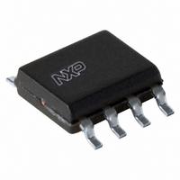
TDA8551T/N1,112 NXP Semiconductors, TDA8551T/N1,112 Datasheet - Page 4

TDA8551T/N1,112
Manufacturer Part Number
TDA8551T/N1,112
Description
IC AMP AUDIO PWR 1.4W MONO 8SOIC
Manufacturer
NXP Semiconductors
Type
Class ABr
Datasheet
1.TDA8551TN1112.pdf
(18 pages)
Specifications of TDA8551T/N1,112
Output Type
1-Channel (Mono)
Package / Case
8-SOIC (3.9mm Width)
Max Output Power X Channels @ Load
1.4W x 1 @ 8 Ohm
Voltage - Supply
2.7 V ~ 5.5 V
Features
Depop, Mute, Short-Circuit and Thermal Protection, Standby, Volume Control
Mounting Type
Surface Mount
Product
Class-AB
Output Power
1.4 W
Available Set Gain
20 dB
Thd Plus Noise
0.15 %
Operating Supply Voltage
5 V
Supply Current
6 mA
Maximum Power Dissipation
800 mW
Maximum Operating Temperature
+ 85 C
Mounting Style
SMD/SMT
Audio Load Resistance
8 Ohms
Input Signal Type
Single
Minimum Operating Temperature
- 40 C
Output Signal Type
Differential
Supply Type
Single
Supply Voltage (max)
5.5 V
Supply Voltage (min)
2.7 V
Lead Free Status / RoHS Status
Lead free / RoHS Compliant
Lead Free Status / RoHS Status
Lead free / RoHS Compliant, Lead free / RoHS Compliant
Other names
568-3477-5
935232730112
TDA8551TD
935232730112
TDA8551TD
NXP Semiconductors
FUNCTIONAL DESCRIPTION
The TDA8551; TDA8551T is a 1 W BTL audio power
amplifier capable of delivering 1 W output power to an 8 Ω
load at THD = 10% using a 5 V power supply. The gain of
the amplifier can be set by the digital volume control. In the
maximum volume setting the gain is 20 dB. Using the
MODE pin the device can be switched to the standby
condition, the mute condition and the normal operating
condition. The device is protected by an internal thermal
shutdown protection mechanism.
Power amplifier
The power amplifier is a Bridge Tied Load (BTL) amplifier
with a complementary CMOS output stage. The total
voltage loss for both output power MOS transistors is
within 1 V and with a 5 V supply and an 8 Ω loudspeaker
an output power of 1 W can be delivered. The total gain of
this power amplifier is internally fixed at 20 dB.
Volume control
The volume control operates as a digital controlled
attenuator between the audio input pin and the power
amplifier. In the maximum volume control setting the
attenuation is 0 dB and in the minimum volume control
setting the typical attenuation is 80 dB. The attenuation
can be set in 64 steps by the UP/DOWN pin.
This UP/DOWN pin is a trinary input:
• Floating UP/DOWN pin: volume remains unchanged
• Negative pulses: setting volume towards minimum
• Positive pulses: setting volume towards maximum.
1998 Feb 23
1 W BTL audio amplifier with digital volume
control
4
Each pulse on the UP/DOWN pin results in a change in
gain of 80/64 = 1.25 dB (typical value). In the basic
application the UP/DOWN pin is switched to ground or V
by a double push-button. When the supply voltage is
initially connected, after a complete removal of the supply,
the initial state of the volume control is an attenuation of
40 dB (low volume), so the gain of the total amplifier is
−20 dB. After powering-up, some positive pulses have to
be applied to the UP/DOWN pin for turning up to listening
volume. When the device is switched with the MODE
select pin to the mute or the standby condition, the volume
control attenuation setting remains on its value, assumed
that the voltage on pin V
supply voltage. After switching the device back to the
operation mode, the previous volume setting is
maintained.
Mode select pin
The device is in the standby mode (with a very low current
consumption) if the voltage at the MODE pin is between V
and V
0.5 V the amplifier is fully operational. In the range
between 1 V and V
condition. The mute condition is useful for using it as a ‘fast
mute’; in this mode output signal is suppressed, while the
volume setting remains at its value. It is advised to keep
the device in the mute condition while the input capacitor
is being charged. This can be done by holding the MODE
pin at a level of 0.5V
before giving the first volume-UP pulses.
P
− 0.5 V. At a mode select voltage level of less than
P
P
− 1.4 V the amplifier is in the mute
, or by waiting approximately 100 ms
P
does not fall below the minimum
Product specification
TDA8551
P
P


