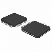
SC16C554IB80,557 NXP Semiconductors, SC16C554IB80,557 Datasheet - Page 26

SC16C554IB80,557
Manufacturer Part Number
SC16C554IB80,557
Description
IC UART QUAD SOT315-1
Manufacturer
NXP Semiconductors
Datasheet
1.SC16C554DIA68512.pdf
(55 pages)
Specifications of SC16C554IB80,557
Number Of Channels
4, QUART
Fifo's
16 Byte
Voltage - Supply
2.5V, 3.3V, 5V
With Auto Flow Control
Yes
With Irda Encoder/decoder
Yes
With False Start Bit Detection
Yes
With Modem Control
Yes
With Cmos
Yes
Mounting Type
Surface Mount
Package / Case
80-LQFP
Lead Free Status / RoHS Status
Lead free / RoHS Compliant
Other names
935270075557
SC16C554IB80
SC16C554IB80
SC16C554IB80
SC16C554IB80
Philips Semiconductors
9397 750 13132
Product data
Table 10:
Table 11:
Bit
2
1
0
FCR[7]
0
0
1
1
Symbol
FCR[2]
FCR[1]
FCR[0]
FIFO Control Register bits description
RCVR trigger levels
Quad UART with 16-byte FIFO and infrared (IrDA) encoder/decoder
FCR[6]
0
1
0
1
Rev. 05 — 10 May 2004
Description
Transmit operation in mode ‘1’: When the SC16C554/554D is in FIFO
mode (FCR[0] = logic 1; FCR[3] = logic 1), the TXRDY pin will be a
logic 1 when the transmit FIFO is completely full. It will be a logic 0 if one
or more FIFO locations are empty.
Receive operation in mode ‘1’: When the SC16C554/554D is in FIFO
mode (FCR[0] = logic 1; FCR[3] = logic 1) and the trigger level has been
reached, or a Receive Time-Out has occurred, the RXRDY pin will go to
a logic 0. Once activated, it will go to a logic 1 after there are no more
characters in the FIFO.
XMIT FIFO reset.
RCVR FIFO reset.
FIFO enable.
Logic 0 = No FIFO transmit reset (normal default condition).
Logic 1 = Clears the contents of the transmit FIFO and resets the
FIFO counter logic (the transmit shift register is not cleared or
altered). This bit will return to a logic 0 after clearing the FIFO.
Logic 0 = No FIFO receive reset (normal default condition).
Logic 1 = Clears the contents of the receive FIFO and resets the FIFO
counter logic (the receive shift register is not cleared or altered). This
bit will return to a logic 0 after clearing the FIFO.
Logic 0 = Disable the transmit and receive FIFO (normal default
condition).
Logic 1 = Enable the transmit and receive FIFO. This bit must be a
‘1’ when other FCR bits are written to, or they will not be
programmed.
RX FIFO trigger level
1
4
8
14
…continued
SC16C554/554D
© Koninklijke Philips Electronics N.V. 2004. All rights reserved.
26 of 55


