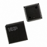
SC16C2552IA44,529 NXP Semiconductors, SC16C2552IA44,529 Datasheet - Page 5

SC16C2552IA44,529
Manufacturer Part Number
SC16C2552IA44,529
Description
IC UART DUAL W/FIFO 44-PLCC
Manufacturer
NXP Semiconductors
Datasheet
1.SC16C2552IA44529.pdf
(38 pages)
Specifications of SC16C2552IA44,529
Features
2 Channels
Number Of Channels
2, DUART
Fifo's
16 Byte
Voltage - Supply
2.5V, 3.3V, 5V
With False Start Bit Detection
Yes
With Modem Control
Yes
With Cmos
Yes
Mounting Type
Surface Mount
Package / Case
44-LCC (J-Lead)
Lead Free Status / RoHS Status
Lead free / RoHS Compliant
Other names
568-1186-5
935270026529
SC16C2552IA44-S
935270026529
SC16C2552IA44-S
Available stocks
Company
Part Number
Manufacturer
Quantity
Price
Company:
Part Number:
SC16C2552IA44,529
Manufacturer:
NXP Semiconductors
Quantity:
10 000
Philips Semiconductors
Table 2:
9397 750 11636
Product data
Symbol
CTSA, CTSB
DSRA, DSRB 41, 29
DTRA, DTRB
RIA, RIB
RTSA, RTSB
RXA, RXB
TXA, TXB
Pin description
Pin
40, 28
37, 27
43, 31
36, 23
39, 25
38, 26
Type
I
I
O
I
O
I
O
…continued
Description
Clear to Send (Active-LOW). These inputs are associated with individual UART
channels, A through B. A logic 0 on the CTS pin indicates the modem or data set is
ready to accept transmit data from the SC16C2552. Status can be tested by reading
MSR[4].
Data Set Ready (Active-LOW). These inputs are associated with individual UART
channels, A through B. A logic 0 on this pin indicates the modem or data set is
powered-on and is ready for data exchange with the UART.
Data Terminal Ready (Active-LOW). These outputs are associated with individual
UART channels, A through B. A logic 0 on this pin indicates that the SC16C2552 is
powered-on and ready. This pin can be controlled via the modem control register.
Writing a logic 1 to MCR[0] will set the DTR output to logic 0, enabling the modem. This
pin will be a logic 1 after writing a logic 0 to MCR[0], or after a reset.
Ring Indicator (Active-LOW). These inputs are associated with individual UART
channels, A through B. A logic 0 on this pin indicates the modem has received a ringing
signal from the telephone line. A logic 1 transition on this input pin will generate an
interrupt.
Request to Send (Active-LOW). These outputs are associated with individual UART
channels, A through B. A logic 0 on the RTS pin indicates the receiver is ready to
receive data. Writing a logic 1 in the modem control register MCR[1] will set this pin to a
logic 0, indicating that the receiver is ready to receive data. After a reset this pin will be
set to a logic 1.
Receive data A, B. These inputs are associated with individual serial channel data to
the SC16C2552 receive input circuits, A-B. The RX signal will be a logic 1 during reset,
idle (no data), or when the transmitter is disabled. During the local loop-back mode, the
RX input pin is disabled and TX data is connected to the UART RX input, internally.
Transmit data A, B. These outputs are associated with individual serial transmit
channel data from the SC16C2552. The TX signal will be a logic 1 during reset, idle (no
data), or when the transmitter is disabled. During the local loop-back mode, the TX
output pin is disabled and TX data is internally connected to the UART RX input.
Rev. 03 — 20 June 2003
Dual UART with 16-byte transmit and receive FIFOs
© Koninklijke Philips Electronics N.V. 2003. All rights reserved.
SC16C2552
5 of 38


