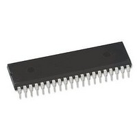
HD3-6402R-9Z Intersil, HD3-6402R-9Z Datasheet - Page 3

HD3-6402R-9Z
Manufacturer Part Number
HD3-6402R-9Z
Description
IC UART CMOS 5V 2MHZ 40-DIP
Manufacturer
Intersil
Datasheet
1.HD3-6402R-9Z.pdf
(7 pages)
Specifications of HD3-6402R-9Z
Features
Low Power CMOS
Number Of Channels
8
Voltage - Supply
4.5 V ~ 5.5 V
With False Start Bit Detection
Yes
With Cmos
Yes
Mounting Type
Through Hole
Package / Case
40-DIP (0.600", 15.24mm)
No. Of Channels
1
Supply Voltage Range
4.5V To 5.5V
Operating Temperature Range
-40°C To +85°C
Digital Ic Case Style
DIP
No. Of Pins
40
Supply Voltage Max
5.5V
Supply Voltage Min
4.5V
Rohs Compliant
Yes
Clock Frequency
2MHz
Operating Temperature Max
85°C
Lead Free Status / RoHS Status
Lead free / RoHS Compliant
Pin Description
PIN TYPE SYMBOL
10
11
12
13
14
15
16
17
18
19
20
21
22
23
1
2
3
4
5
6
7
8
9
O
O
O
O
O
O
O
O
O
O
O
O
O
I
I
I
I
I
I
I
V
RBR8
RBR7
RBR6
RBR5
RBR4
RBR3
RBR2
RBR1
TBRE
TBRL
GND
RRD
RRC
DRR
SFD
RRI
MR
CC
NC
PE
OE
DR
FE
†
Positive Voltage Supply
No Connection
Ground
A high level on RECEIVER REGISTER DISABLE
forces the receiver holding out-puts RBR1-RBR8
to high impedance state.
The contents of the RECEIVER BUFFER REGIS-
TER appear on these three-state outputs. Word for-
mats less than 8 characters are right justified to
RBR1.
See Pin 5-RBR8
See Pin 5-RBR8
See Pin 5-RBR8
See Pin 5-RBR8
See Pin 5-RBR8
See Pin 5-RBR8
See Pin 5-RBR8
A high level on PARITY ERROR indicates received
parity does not match parity programmed by control
bits. When parity is inhibited this output is low.
A high level on FRAMING ERROR indicates the
first stop bit was invalid.
A high level on OVERRUN ERROR indicates the
data received flag was not cleared before the last
character was transferred to the receiver buffer
register.
A high level on STATUS FLAGS DISABLE forces
the outputs PE, FE, OE, DR, TBRE to a high im-
pedance state.
The Receiver register clock is 16X the receiver
data rate.
A low level on DATA RECEIVED RESET clears
the data received output DR to a low level.
A high level on DATA RECEIVED indicates a
character has been received and transferred to
the receiver buffer register.
Serial data on RECEIVER REGISTER INPUT is
clocked into the receiver register.
A high level on MASTER RESET clears PE, FE,
OE and DR to a low level and sets the transmitter
register empty (TRE) to a high level 18 clock cycles
after MR falling edge. MR does not clear the receiv-
er buffer register. This input must be pulsed at least
once after power up. The HD-6402 must be master
reset after power up. The reset pulse should meet
V
edge of MR before beginning operation.
A high level on TRANSMITTER BUFFER REGIS-
TER EMPTY indicates the transmitter buffer register
has transferred its data to the transmitter register
and is ready for new data.
A low level on TRANSMITTER BUFFER REGIS-
TER LOAD transfers data from inputs TBR1-
TBR8 into the transmitter buffer register. A low to
high transition on TBRL initiates data transfer to
the transmitter register. If busy, transfer is auto-
matically delayed so that the two characters are
transmitted end to end.
IH
and t
MR
. Wait 18 clock cycles after the falling
3
DESCRIPTION
HD-6402
HD-6402
PIN TYPE SYMBOL
† A 0.1µF decoupling capacitor from the V
24
25
26
27
28
29
30
31
32
33
34
35
36
37
38
39
40
recommended.
O
O
I
I
I
I
I
I
I
I
I
I
I
I
I
I
I
TRB1
TBR2
TBR3
TBR4
TBR5
TBR6
TBR7
TBR8
CLS2
CLS1
TRO
TRC
TRE
CRL
SBS
EPE
PI
A high level on TRANSMITTER REGISTER EMP-
TY indicates completed transmission of a charac-
ter including stop bits.
Character data, start data and stop bits appear se-
rially at the TRANSMITTER REGISTER OUTPUT.
Character data is loaded into the TRANSMITTER
BUFFER REGISTER via inputs TBR1-TBR8. For
character formats less than 8 bits the TBR8, 7 and
6 inputs are ignored corresponding to their pro-
grammed word length.
See Pin 26-TBR1.
See Pin 26-TBR1.
See Pin 26-TBR1.
See Pin 26-TBR1.
See Pin 26-TBR1.
See Pin 26-TBR1.
See Pin 26-TBR1.
A high level on CONTROL REGISTER LOAD
loads the control register with the control word. The
control word is latched on the falling edge of CRL.
CRL may be tied high.
A high level on PARITY INHIBIT inhibits parity gen-
eration, parity checking and forces PE output low.
A high level on STOP BIT SELECT selects 1.5
stop bits for 5 character format and 2 stop bits for
other lengths.
These inputs program the CHARACTER
LENGTH SELECTED (CLS1 low CLS2 low 5 bits)
(CLS1 high CLS2 low 6 bits) (CLS1 low CLS2
high 7 bits) (CLS1 high CLS2 high 8 bits.)
See Pin 37-CLS2.
When PI is low, a high level on EVEN PARITY
ENABLE generates and checks even parity. A low
level selects odd parity.
The TRANSMITTER REGISTER CLOCK is 16X
the transmit data rate.
DESCRIPTION
CC
pin to the GND is


