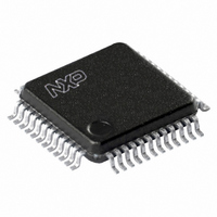
SC68C752BIB48,157 NXP Semiconductors, SC68C752BIB48,157 Datasheet - Page 16

SC68C752BIB48,157
Manufacturer Part Number
SC68C752BIB48,157
Description
IC UART DUAL 48LQFP
Manufacturer
NXP Semiconductors
Datasheet
1.SC68C752BIBS128.pdf
(48 pages)
Specifications of SC68C752BIB48,157
Number Of Channels
2, DUART
Package / Case
48-LQFP
Fifo's
64 Byte
Voltage - Supply
2.5V, 3.3V, 5V
With Auto Flow Control
Yes
With False Start Bit Detection
Yes
With Modem Control
Yes
Mounting Type
Surface Mount
Data Rate
5 Mbps
Supply Voltage (max)
5.5 V
Supply Voltage (min)
2.25 V
Supply Current
4.5 mA
Maximum Operating Temperature
+ 85 C
Minimum Operating Temperature
- 40 C
Mounting Style
SMD/SMT
Operating Supply Voltage
2.5 V or 3.3 V or 5 V
Lead Free Status / RoHS Status
Lead free / RoHS Compliant
Lead Free Status / RoHS Status
Lead free / RoHS Compliant, Lead free / RoHS Compliant
Other names
935278767157
SC68C752BIB48
SC68C752BIB48
SC68C752BIB48
SC68C752BIB48
Available stocks
Company
Part Number
Manufacturer
Quantity
Price
Company:
Part Number:
SC68C752BIB48,157
Manufacturer:
NXP Semiconductors
Quantity:
10 000
NXP Semiconductors
SC68C752B_4
Product data sheet
6.6.2.1 Transmitter
6.6.2.2 Receiver
6.6.2 Block DMA transfers (DMA mode 1)
6.7 Sleep mode
Figure 11
TXRDYn is active when there is a trigger level number of spaces available. It becomes
inactive when the FIFO is full.
RXRDYn becomes active when the trigger level has been reached, or when a time-out
interrupt occurs. It will go inactive when the FIFO is empty or an error in the receive FIFO
is flagged by LSR[7].
Sleep mode is an enhanced feature of the SC68C752B UART. It is enabled when EFR[4],
the enhanced functions bit, is set and when IER[4] is set. Sleep mode is entered when:
Remark: Sleep mode will not be entered if there is data in the receive FIFO.
In Sleep mode, the UART clock and baud rate clock are stopped. Since most registers are
clocked using these clocks, the power consumption is greatly reduced. The UART will
wake up when any change is detected on the RXn line, when there is any change in the
state of the modem input pins, or if data is written to the transmit FIFO.
Remark: Writing to the divisor latches, DLL and DLM, to set the baud clock, must not be
done during Sleep mode. Therefore, it is advisable to disable Sleep mode using IER[4]
before writing to DLL or DLM.
Fig 11. TXRDYn and RXRDYn in DMA mode 1
•
•
•
The serial data input line, RXn, is idle (see
conditions”).
The transmit FIFO and transmit shift register are empty.
There are no interrupts pending except THR and time-out interrupts.
trigger
wrptr
wrptr
level
shows TXRDYn and RXRDYn in DMA mode 1.
transmit
5 V, 3.3 V and 2.5 V dual UART, 5 Mbit/s (max.), with 64-byte FIFOs
Rev. 04 — 20 January 2010
FIFO full
TXRDYn
TXRDYn
Section 6.8 “Break and time-out
trigger
rdptr
rdptr
level
FIFO EMPTY
receive
SC68C752B
at least one
location filled
© NXP B.V. 2010. All rights reserved.
RXRDYn
RXRDYn
002aaa234
16 of 48


