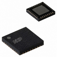
SC16C850VIBS,128 NXP Semiconductors, SC16C850VIBS,128 Datasheet - Page 25

SC16C850VIBS,128
Manufacturer Part Number
SC16C850VIBS,128
Description
IC UART SINGLE W/FIFO 32-HVQFN
Manufacturer
NXP Semiconductors
Datasheet
1.SC16C850VIBS128.pdf
(48 pages)
Specifications of SC16C850VIBS,128
Features
Programmable
Number Of Channels
1, UART
Fifo's
128 Byte
Protocol
RS485
Voltage - Supply
1.8V
With Auto Flow Control
Yes
With Irda Encoder/decoder
Yes
With False Start Bit Detection
Yes
With Modem Control
Yes
With Cmos
Yes
Mounting Type
Surface Mount
Package / Case
32-VFQFN Exposed Pad
Transmitter And Receiver Fifo Counter
Yes
Data Rate
5Mbps
Mounting
Surface Mount
Pin Count
32
Operating Temperature (min)
-40C
Operating Temperature (max)
85C
Operating Temperature Classification
Industrial
Lead Free Status / RoHS Status
Lead free / RoHS Compliant
Other names
935283087128
SC16C850VIBS-F
SC16C850VIBS-F
SC16C850VIBS-F
SC16C850VIBS-F
NXP Semiconductors
SC16C850V
Product data sheet
7.6 Modem Control Register (MCR)
Table 17.
This register controls the interface with the modem or a peripheral device.
Table 18.
LCR[1]
0
0
1
1
Bit
7
6
5
3
2
1
0
4
Symbol
MCR[7]
MCR[6]
MCR[5]
MCR[4]
MCR[3]
MCR[2]
MCR[1]
MCR[0]
LCR[1:0] word length
Modem Control Register bits description
LCR[0]
0
1
0
1
Single UART with 128-byte FIFOs, IrDA, and XScale VLIO bus interface
All information provided in this document is subject to legal disclaimers.
Description
Clock select
IR enable (see
Interrupt type.
Loopback. Enable the local Loopback mode (diagnostics). In this mode the
transmitter output (TX) and the receiver input (RX), CTS, DSR, CD, and RI are
disconnected from the SC16C850V I/O pins. Internally the modem data and
control pins are connected into a loopback data configuration (see
this mode, the receiver and transmitter interrupts remain fully operational. The
Modem Control Interrupts are also operational, but the interrupts’ sources are
switched to the lower four bits of the Modem Control. Interrupts continue to be
controlled by the IER register.
OP2. This bit is used for internal Loopback mode only. In Loopback mode, this
bit is used to write the state of the modem CD interface signal.
OP1. This bit is used for internal Loopback mode only. In Loopback mode, this
bit is used to write the state of the modem RI interface signal.
RTS
DTR
logic 0 = divide-by-1 clock input
logic 1 = divide-by-4 clock input
logic 0 = enable the standard modem receive and transmit input/output
interface (normal default condition)
logic 1 = enable infrared IrDA receive and transmit inputs/outputs. While in
this mode, the TX/RX output/inputs are routed to the infrared
encoder/decoder. The data input and output levels will conform to the IrDA
infrared interface requirement. As such, while in this mode, the infrared TX
output will be a logic 0 during idle data conditions.
logic 0 = CMOS output
logic 1 = open-source. A 300 Ω to 500 Ω pull-down resistor is required.
logic 0 = disable Loopback mode (normal default condition)
logic 1 = enable local Loopback mode (diagnostics)
logic 0 = force RTS output to a logic 1 (normal default condition)
logic 1 = force RTS output to a logic 0
logic 0 = force DTR output to a logic 1 (normal default condition)
logic 1 = force DTR output to a logic 0
Rev. 5 — 19 January 2011
Figure
Word length (bits)
5
6
7
8
14).
SC16C850V
© NXP B.V. 2011. All rights reserved.
Figure
25 of 48
6). In


