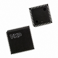
SC28L92A1A,512 NXP Semiconductors, SC28L92A1A,512 Datasheet - Page 14

SC28L92A1A,512
Manufacturer Part Number
SC28L92A1A,512
Description
IC UART DUAL W/FIFO 44-PLCC
Manufacturer
NXP Semiconductors
Series
IMPACTr
Datasheet
1.SC28L92A1B557.pdf
(73 pages)
Specifications of SC28L92A1A,512
Features
False-start Bit Detection
Number Of Channels
2, DUART
Fifo's
16 Byte
Voltage - Supply
3.3V, 5V
With Auto Flow Control
Yes
With False Start Bit Detection
Yes
With Modem Control
Yes
With Cmos
Yes
Mounting Type
Surface Mount
Package / Case
44-LCC (J-Lead)
Lead Free Status / RoHS Status
Lead free / RoHS Compliant
Other names
935263293512
SC28L92A1A
SC28L92A1A
SC28L92A1A
SC28L92A1A
Available stocks
Company
Part Number
Manufacturer
Quantity
Price
Company:
Part Number:
SC28L92A1A,512
Manufacturer:
NXP Semiconductors
Quantity:
10 000
NXP Semiconductors
SC28L92_7
Product data sheet
6.1.4 FIFO configuration
6.1.5 68xxx mode
6.2.1 Crystal clock
6.2 Timing circuits
receivers, and counter/timer. When OP3 to OP7 are programmed as interrupts, their
output buffers are changed to the open-drain active LOW configuration. The OP pins may
be used for DMA and modem control as well (see
Each receiver and transmitter has a 16 byte FIFO. These FIFOs may be configured to
operate at a fill capacity of either 8 bytes or 16 bytes. This feature may be used if it is
desired to operate the SC28L92 in strict compliance with the SC26C92. The 8 byte or
16 byte mode is controlled by the MR0A[3] bit. A logic 0 value for this bit sets the 8-bit
mode (the default); a logic 1 sets the 16 byte mode. MR0A bit 3 sets the FIFO size for both
channels.
The FIFO fill interrupt level automatically follow the programming of the MR0A[3] bit. See
Table 25
When the I/M pin is connected to GND (ground), the operation of the SC28L92 switches to
the bus interface compatible with the Motorola bus interfaces. Several of the pins change
their function as follows:
The interrupt vector is enabled and the interrupt vector will be placed on the data bus
when IACKN is asserted LOW. The interrupt vector register is located at address 0xC. The
contents of this register are set to 0x0F on the application of RESETN.
The generation of DACKN uses two positive edges of the X1 clock as the DACKN delay
from the falling edge of CEN. If the CEN is withdrawn before two edges of the X1 clock
occur, the generation of DACKN is terminated. Systems not strictly requiring DACKN
may use the 68xxx mode with the bus timing of the 80xxx mode greatly decreasing the
bus cycle time.
The timing block consists of a crystal oscillator, a baud rate generator, a programmable
16-bit counter/timer, and four clock selectors. The crystal oscillator operates directly from
a crystal connected across the X1/CLK and X2 inputs. If an external clock of the
appropriate frequency is available, it may be connected to X1/CLK. The clock serves as
the basic timing reference for the Baud Rate Generator (BRG), the counter/timer, and
other internal circuits. A clock signal within the limits specified in
characteristics”
instead of a crystal, X1 should be driven using a configuration similar to the one in
Figure
IP6 becomes IACKN input
RDN becomes DACKN
WRN becomes R/WN
17. Nominal crystal rate is 3.6864 MHz. Rates up to 8 MHz may be used.
and
Table
must always be supplied to the DUART. If an external clock is used
26.
Rev. 07 — 19 December 2007
3.3 V/5.0 V Dual Universal Asynchronous Receiver/Transmitter
Section
7.4).
Section 10 “Dynamic
SC28L92
© NXP B.V. 2007. All rights reserved.
14 of 73


