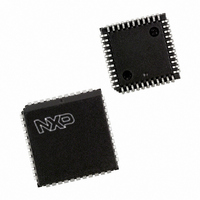
SC28L92A1A,529 NXP Semiconductors, SC28L92A1A,529 Datasheet - Page 50

SC28L92A1A,529
Manufacturer Part Number
SC28L92A1A,529
Description
IC UART DUAL W/FIFO 44-PLCC
Manufacturer
NXP Semiconductors
Series
IMPACTr
Datasheet
1.SC28L92A1B557.pdf
(73 pages)
Specifications of SC28L92A1A,529
Features
False-start Bit Detection
Number Of Channels
2, DUART
Fifo's
16 Byte
Voltage - Supply
3.3V, 5V
With Auto Flow Control
Yes
With False Start Bit Detection
Yes
With Modem Control
Yes
With Cmos
Yes
Mounting Type
Surface Mount
Package / Case
44-LCC (J-Lead)
Lead Free Status / RoHS Status
Lead free / RoHS Compliant
Other names
568-1188-5
935263293529
SC28L92A1A-S
935263293529
SC28L92A1A-S
Available stocks
Company
Part Number
Manufacturer
Quantity
Price
Company:
Part Number:
SC28L92A1A,529
Manufacturer:
NXP Semiconductors
Quantity:
10 000
NXP Semiconductors
8. Limiting values
SC28L92_7
Product data sheet
MR2[4] is the bit that allows the transmitter to be controlled by the CTS pin (IP0 or IP1).
When this bit is set to one AND the CTS input is driven HIGH, the transmitter will stop
sending data at the end of the present character being serialized. It is usually the RTS
output of the receiver that will be connected to the transmitter’s CTS input. The receiver
will set RTS HIGH when the receiver FIFO is full AND the start bit of the 9th or 17th
character is sensed. Transmission then stops with 9 or 17 valid characters in the receiver.
When MR2[4] is set to one, CTSN must be at zero for the transmitter to operate. If MR2[4]
is set to zero, the IP pin will have no effect on the operation of the transmitter. MR1[7] is
the bit that allows the receiver to control OP0. When OP0 (or OP1) is controlled by the
receiver, the meaning of that pin will be.
Table 64.
In accordance with the Absolute Maximum Rating System (IEC 60134).
[1]
[2]
[3]
Symbol Parameter
T
T
V
V
P
P
amb
stg
CC
S
D
der
For operation at elevated temperatures, the device must be derated based on 150 C maximum junction
temperature.
Parameters are valid over specified temperature range.
This product includes circuitry specifically designed for the protection of its internal devices from damaging
effects of excessive static charge. Nonetheless, it is suggested that conventional precautions be taken to
avoid applying any voltages larger than the rated maxima.
ambient temperature
storage temperature
voltage from V
voltage from any pin to GND
package power dissipation
dissipation derating factor
Limiting values
PLCC44
QFP44
HVQFN48
PLCC44
QFP44
HVQFN48
Rev. 07 — 19 December 2007
3.3 V/5.0 V Dual Universal Asynchronous Receiver/Transmitter
CC
to GND
Conditions
above 25 C
[1][2]
[3]
[3]
Min
-
-
-
-
-
-
40
65
0.5
0.5
SC28L92
© NXP B.V. 2007. All rights reserved.
Max
+85
+150
+7.0
V
2.4
1.78
0.5
19
14
28
CC
+ 0.5 V
Unit
V
W
W
W
mW/ C
mW/ C
mW/ C
50 of 73
C
C


