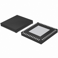
SC16C654BIBS,528 NXP Semiconductors, SC16C654BIBS,528 Datasheet - Page 17

SC16C654BIBS,528
Manufacturer Part Number
SC16C654BIBS,528
Description
IC QUAD UART 64BYTE 48HVQFN
Manufacturer
NXP Semiconductors
Datasheet
1.SC16C654BIBS528.pdf
(58 pages)
Specifications of SC16C654BIBS,528
Features
False-start Bit Detection
Number Of Channels
4, QUART
Fifo's
64 Byte
Voltage - Supply
2.5V, 3.3V, 5V
With Auto Flow Control
Yes
With Irda Encoder/decoder
Yes
With False Start Bit Detection
Yes
With Modem Control
Yes
With Cmos
Yes
Mounting Type
Surface Mount
Package / Case
48-VQFN Exposed Pad, 48-HVQFN, 48-SQFN, 48-DHVQFN
Lead Free Status / RoHS Status
Lead free / RoHS Compliant
Other names
935279073528
SC16C654BIBS-F
SC16C654BIBS-F
SC16C654BIBS-F
SC16C654BIBS-F
Philips Semiconductors
9397 750 14965
Product data sheet
6.2 Internal registers
6.3 FIFO operation
The SC16C654B/654DB provides 17 internal registers for monitoring and control. These
registers are shown in
the standard 16C554. These registers function as data holding registers (THR/RHR),
interrupt status and control registers (IER/ISR), a FIFO control register (FCR), line status
and control registers (LCR/LSR), modem status and control registers (MCR/MSR),
programmable data rate (clock) control registers (DLL/DLM), and a user accessible
scratchpad register (SPR). Beyond the general 16C554 features and capabilities, the
SC16C654B/654DB offers an enhanced feature register set (EFR, Xon/Xoff1-2) that
provides on-board hardware/software flow control. Register functions are more fully
described in the following paragraphs.
Table 5:
[1]
[2]
[3]
The 64-byte transmit and receive data FIFOs are enabled by the FIFO Control Register
(FCR) bit 0. With SC16C554 devices, the user can set the receive trigger level, but not the
transmit trigger level. The SC16C654B/654DB provides independent trigger levels for both
receiver and transmitter. To remain compatible with SC16C554, the transmit interrupt
trigger level is set to 8 following a reset. It should be noted that the user can set the
transmit trigger levels by writing to the FCR register, but activation will not take place until
EFR[4] is set to a logic 1. The receiver FIFO section includes a time-out function to ensure
data is delivered to the external CPU. An interrupt is generated whenever the Receive
A2
General register set (THR/RHR, IER/ISR, MCR/MSR, FCR, LSR, SPR)
0
0
0
0
1
1
1
1
Baud rate register set (DLL/DLM)
0
0
Enhanced register set (EFR, Xon/off 1-2)
0
1
1
1
1
These registers are accessible only when LCR[7] is a logic 0.
These registers are accessible only when LCR[7] is a logic 1.
Enhanced Feature Register, Xon1, 2 and Xoff1, 2 are accessible only when the LCR is set to ‘BFh’.
A1
0
0
1
1
0
0
1
1
0
0
1
0
0
1
1
Internal registers decoding
A0
0
1
0
1
0
1
0
1
0
1
0
0
1
0
1
5 V, 3.3 V and 2.5 V quad UART, 5 Mbit/s (max.) with 64-byte FIFOs
Table
Read mode
Receive Holding Register
Interrupt Enable Register
Interrupt Status Register
Line Control Register
Modem Control Register
Line Status Register
Modem Status Register
Scratchpad Register
LSB of Divisor Latch
MSB of Divisor Latch
Enhanced Feature Register
Xon1 word
Xon2 word
Xoff1 word
Xoff2 word
Rev. 02 — 20 June 2005
5. Twelve registers are similar to those already available in
[2]
[3]
SC16C654B/654DB
Write mode
Transmit Holding Register
Interrupt Enable Register
FIFO Control Register
Line Control Register
Modem Control Register
n/a
n/a
Scratchpad Register
LSB of Divisor Latch
MSB of Divisor Latch
Enhanced Feature Register
Xon1 word
Xon2 word
Xoff1 word
Xoff2 word
© Koninklijke Philips Electronics N.V. 2005. All rights reserved.
[1]
17 of 58


