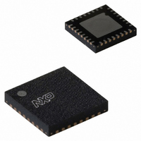
SC68C752BIBS,151 NXP Semiconductors, SC68C752BIBS,151 Datasheet - Page 25

SC68C752BIBS,151
Manufacturer Part Number
SC68C752BIBS,151
Description
IC UART DUAL W/FIFO 32-HVQFN
Manufacturer
NXP Semiconductors
Datasheet
1.SC68C752BIBS151.pdf
(48 pages)
Specifications of SC68C752BIBS,151
Number Of Channels
2, DUART
Fifo's
64 Byte
Voltage - Supply
2.5V, 3.3V, 5V
With Auto Flow Control
Yes
With False Start Bit Detection
Yes
With Modem Control
Yes
Mounting Type
Surface Mount
Package / Case
32-VFQFN Exposed Pad
Lead Free Status / RoHS Status
Lead free / RoHS Compliant
Other names
568-3299
935280969151
SC68C752BIBS-S
935280969151
SC68C752BIBS-S
NXP Semiconductors
SC68C752B_4
Product data sheet
7.6 Modem Control Register (MCR)
Remark: The three error bits (parity, framing, break) may not be updated correctly in the
first read of the LSR when the input clock (XTAL1) is running faster than 36 MHz.
However, the second read is always correct. It is strongly recommended that when using
this device with a clock faster than 36 MHz, that the LSR be read twice and only the
second read be used for decision making. All other bits in the LSR are correct on all
reads.
The MCR controls the interface with the mode, data set, or peripheral device that is
emulating the modem.
Table 15.
[1]
Bit
7
6
5
4
3
2
1
0
MCR[7:5] can only be modified when EFR[4] is set, that is, EFR[4] is a write enable.
Symbol
MCR[7]
MCR[6]
MCR[5]
MCR[4]
MCR[3]
MCR[2]
MCR[1]
MCR[0]
Modem Control Register bits description
[1]
[1]
[1]
5 V, 3.3 V and 2.5 V dual UART, 5 Mbit/s (max.), with 64-byte FIFOs
Description
Clock select.
TCR and TLR enable.
Xon Any.
Enable loopback.
OPA/OPB control.
FIFO Ready enable.
RTS
DTR
Rev. 04 — 20 January 2010
Table 15
logic 0 = divide-by-1 clock input
logic 1 = divide-by-4 clock input
logic 0 = no action.
logic 1 = enable access to the TCR and TLR registers
logic 0 = disable Xon Any function
logic 1 = enable Xon Any function
logic 0 = normal operating mode
logic 1 = Enable local Loopback mode (internal). In this mode the
MCR[3:0] signals are looped back into MSR[7:4] and the TXn output is
looped back to the RXn input internally.
logic 0 = forces OPA/OPB output to HIGH state
logic 1 = forces OPA/OPB output to LOW state. In Loopback mode,
controls MSR[7].
logic 0 = Disable the FIFO Rdy register
logic 1 = Enable the FIFO Rdy register. In Loopback mode, controls
MSR[6].
logic 0 = force RTSn output to inactive (HIGH)
logic 1 = force RTSn output to active (LOW). In Loopback mode,
controls MSR[4]. If auto-RTS is enabled, the RTSn output is controlled
by hardware flow control.
logic 0 = force DTRn output to inactive (HIGH)
logic 1 = force DTRn output to active (LOW). In Loopback mode,
controls MSR[5].
shows Modem Control Register bit settings.
SC68C752B
© NXP B.V. 2010. All rights reserved.
25 of 48


