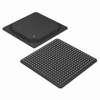
DS3172+ Maxim Integrated Products, DS3172+ Datasheet - Page 40

DS3172+
Manufacturer Part Number
DS3172+
Description
IC TXRX DS3/E3 DUAL 400-BGA
Manufacturer
Maxim Integrated Products
Datasheet
1.DS3171N.pdf
(234 pages)
Specifications of DS3172+
Function
Single-Chip Transceiver
Interface
DS3, E3
Number Of Circuits
2
Voltage - Supply
3.135 V ~ 3.465 V
Current - Supply
328mA
Operating Temperature
0°C ~ 70°C
Mounting Type
Surface Mount
Package / Case
400-BGA
Includes
DS3 Framers, E3 Framers, HDLC Controller, On-Chip BERTs
Lead Free Status / RoHS Status
Lead free / RoHS Compliant
Power (watts)
-
- Current page: 40 of 234
- Download datasheet (2Mb)
Figure 8-10
Figure 8-10. DS3 Framing Transmit Overhead Port Timing
Figure 8-11
Figure 8-11. E3 G.751 Framing Transmit Overhead Port Timing
Figure 8-12
Figure 8-12. E3 G.832 Framing Transmit Overhead Port Timing
8.3.3
8.3.3.1
The TSERn pin is used to input DS3 or E3 payload data bits in all framing modes as well as the C-bits, which can
be treated as payload, in DS3 M23 and E3 G.751 framing modes. The TDENn signal is used to determine the DS3
or E3 payload bit positions on TSERn. The TDENn signal goes high three clocks before the first bit of a payload
sequence is clocked into the TSERn pin and it goes low three clocks before the payload sequence is stopped
being clocked in to the TSERn pin. The TSOFOn signal pulses high three clocks before the start of the DS3 or E3
overhead bit position on TSERn. The TSOFIn pin is used to set the DS3 or E3 frame position. When the TSOFIn
pin transitions low to high, the first DS3/E3 overhead bit position on TSERn will be forced to align to it
Figure 8-13
TOHCLK
TOHCLK
TOHSOF
TOHSOF
TOHCLK
TOHSOF
TOHEN
TOHEN
TOHEN
TOH
TOH
TOH
DS3/E3 Serial Data Interface
DS3/E3 SCT Mode Transmit Serial Interface Pin Functional Timing
shows the relationship between the DS3 transmit overhead port pins.
shows the relationship between the E3 G.751 transmit overhead port pins.
shows the relationship between the E3 G.832 transmit overhead port pins.
to
FAS
1
1
GC
10
Figure 8-15
6
F73
1
2
2
GC
C73
2
A
7
3
3
GC
F74
3
N
8
FAS
4
FA1
4
show the relationship between the SCT transmit port pins.
4
1
1
X1
FAS
5
FA1
5
5
2
2
F11
FAS
6
FA1
6
C11
6
3
3
FAS
7
FA1
7
F12
7
4
4
FAS
8
FA1
8
C12
8
5
5
FAS
9
FA1
9
F13
9
6
6
10
10
FAS
10
FA1
C13
7
7
11
11
11
FAS
FA1
F14
8
8
40
12
12
12
FAS
FA2
1
X2
9
13
13
13
FAS
FA2
F21
10
2
14
14
14
FA2
C21
A
3
15
15
15
FA2
F22
N
4
16
16
16
FAS
FA2
C22
1
5
17
17
17
FAS
FA2
F23
2
6
18
18
18
FAS
FA2
C23
3
7
19
19
19
FAS
FA2
F24
4
8
20
20
20
FAS
P1
E M
5
1
21
21
21
FAS
F31
E M
6
2
22
22
22
FAS
C31
E M
8
3
23
23
23
FAS
E M
F32
9
4
24
C32
FAS
24
24
E M
9
5
Related parts for DS3172+
Image
Part Number
Description
Manufacturer
Datasheet
Request
R

Part Number:
Description:
MAX7528KCWPMaxim Integrated Products [CMOS Dual 8-Bit Buffered Multiplying DACs]
Manufacturer:
Maxim Integrated Products
Datasheet:

Part Number:
Description:
Single +5V, fully integrated, 1.25Gbps laser diode driver.
Manufacturer:
Maxim Integrated Products
Datasheet:

Part Number:
Description:
Single +5V, fully integrated, 155Mbps laser diode driver.
Manufacturer:
Maxim Integrated Products
Datasheet:

Part Number:
Description:
VRD11/VRD10, K8 Rev F 2/3/4-Phase PWM Controllers with Integrated Dual MOSFET Drivers
Manufacturer:
Maxim Integrated Products
Datasheet:

Part Number:
Description:
Highly Integrated Level 2 SMBus Battery Chargers
Manufacturer:
Maxim Integrated Products
Datasheet:

Part Number:
Description:
Current Monitor and Accumulator with Integrated Sense Resistor; ; Temperature Range: -40°C to +85°C
Manufacturer:
Maxim Integrated Products

Part Number:
Description:
TSSOP 14/A�/RS-485 Transceivers with Integrated 100O/120O Termination Resis
Manufacturer:
Maxim Integrated Products

Part Number:
Description:
TSSOP 14/A�/RS-485 Transceivers with Integrated 100O/120O Termination Resis
Manufacturer:
Maxim Integrated Products

Part Number:
Description:
QFN 16/A�/AC-DC and DC-DC Peak-Current-Mode Converters with Integrated Step
Manufacturer:
Maxim Integrated Products

Part Number:
Description:
TDFN/A/65V, 1A, 600KHZ, SYNCHRONOUS STEP-DOWN REGULATOR WITH INTEGRATED SWI
Manufacturer:
Maxim Integrated Products

Part Number:
Description:
Integrated Temperature Controller f
Manufacturer:
Maxim Integrated Products

Part Number:
Description:
SOT23-6/I�/45MHz to 650MHz, Integrated IF VCOs with Differential Output
Manufacturer:
Maxim Integrated Products

Part Number:
Description:
SOT23-6/I�/45MHz to 650MHz, Integrated IF VCOs with Differential Output
Manufacturer:
Maxim Integrated Products

Part Number:
Description:
EVALUATION KIT/2.4GHZ TO 2.5GHZ 802.11G/B RF TRANSCEIVER WITH INTEGRATED PA
Manufacturer:
Maxim Integrated Products

Part Number:
Description:
QFN/E/DUAL PCIE/SATA HIGH SPEED SWITCH WITH INTEGRATED BIAS RESISTOR
Manufacturer:
Maxim Integrated Products
Datasheet:


