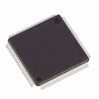
DS2155LC2+ Maxim Integrated Products, DS2155LC2+ Datasheet - Page 204

DS2155LC2+
Manufacturer Part Number
DS2155LC2+
Description
IC TXRX T1/E1/J1 SGL 100-LQFP
Manufacturer
Maxim Integrated Products
Datasheet
1.DS2155L.pdf
(238 pages)
Specifications of DS2155LC2+
Function
Single-Chip Transceiver
Interface
E1, HDLC, J1, T1
Number Of Circuits
1
Voltage - Supply
3.14 V ~ 3.47 V
Current - Supply
75mA
Operating Temperature
0°C ~ 70°C
Mounting Type
Surface Mount
Package / Case
100-LQFP
Includes
BERT Generator and Detector, CMI Coder and Decoder, HDLC Controller
Lead Free Status / RoHS Status
Lead free / RoHS Compliant
Power (watts)
-
- Current page: 204 of 238
- Download datasheet (2Mb)
Table 34-B. ID Code Structure
Table 34-C. Device ID Codes
34.3 Test Registers
IEEE 1149.1 requires a minimum of two test registers, the boundary scan register and the bypass register.
An optional test register, the identification register, has been included with the DS2155 design. It is used
with the IDCODE instruction and the Test-Logic-Reset state of the TAP controller.
34.4 Boundary Scan Register
This register contains both a shift register path and a latched parallel output for all control cells and digital
I/O cells. It is n bits in length. See
34.5 Bypass Register
This is a single one-bit shift register used with the BYPASS, CLAMP, and HIGH-Z instructions that
provides a short path between JTDI and JTDO.
34.6 Identification Register
The identification register contains a 32-bit shift register and a 32-bit latched parallel output. This register
is selected during the IDCODE instruction and when the TAP controller is in the Test-Logic-Reset state.
See
MSB
Version
Contact Factory
4 bits
DS2155
DS2156
DS21354
DS21554
DS21352
DS21552
Table 34-B
PART
and
Device ID
16 bits
Table 34-C
16-BIT ID
0010h
0019h
0005h
0003h
0004h
0002h
JEDEC
00010100001
for more information on bit usage.
Table 34-D
for cell bit locations and definitions.
204 of 238
LSB
1
1
Related parts for DS2155LC2+
Image
Part Number
Description
Manufacturer
Datasheet
Request
R

Part Number:
Description:
IC TXRX T1/E1/J1 1-CHIP 100-LQFP
Manufacturer:
Maxim Integrated Products
Datasheet:

Part Number:
Description:
IC TXRX T1/E1/J1 1-CHIP 100-LQFP
Manufacturer:
Maxim Integrated Products
Datasheet:

Part Number:
Description:
Manufacturer:
Maxim Integrated Products
Datasheet:

Part Number:
Description:
Ds2155 T1/e1/j1 Single-chip Transceiver
Manufacturer:
Maxim Integrated Products, Inc.
Datasheet:

Part Number:
Description:
power light source Luxeon Line
Manufacturer:
LUMILEDS [Lumileds Lighting Company]
Datasheet:

Part Number:
Description:
MAX7528KCWPMaxim Integrated Products [CMOS Dual 8-Bit Buffered Multiplying DACs]
Manufacturer:
Maxim Integrated Products
Datasheet:

Part Number:
Description:
Single +5V, fully integrated, 1.25Gbps laser diode driver.
Manufacturer:
Maxim Integrated Products
Datasheet:

Part Number:
Description:
Single +5V, fully integrated, 155Mbps laser diode driver.
Manufacturer:
Maxim Integrated Products
Datasheet:

Part Number:
Description:
VRD11/VRD10, K8 Rev F 2/3/4-Phase PWM Controllers with Integrated Dual MOSFET Drivers
Manufacturer:
Maxim Integrated Products
Datasheet:

Part Number:
Description:
Highly Integrated Level 2 SMBus Battery Chargers
Manufacturer:
Maxim Integrated Products
Datasheet:

Part Number:
Description:
Current Monitor and Accumulator with Integrated Sense Resistor; ; Temperature Range: -40°C to +85°C
Manufacturer:
Maxim Integrated Products

Part Number:
Description:
TSSOP 14/A°/RS-485 Transceivers with Integrated 100O/120O Termination Resis
Manufacturer:
Maxim Integrated Products

Part Number:
Description:
TSSOP 14/A°/RS-485 Transceivers with Integrated 100O/120O Termination Resis
Manufacturer:
Maxim Integrated Products

Part Number:
Description:
QFN 16/A°/AC-DC and DC-DC Peak-Current-Mode Converters with Integrated Step
Manufacturer:
Maxim Integrated Products


