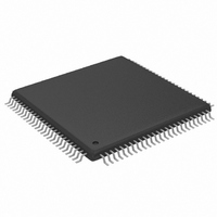
MAX9675ECQ+ Maxim Integrated Products, MAX9675ECQ+ Datasheet - Page 22

MAX9675ECQ+
Manufacturer Part Number
MAX9675ECQ+
Description
IC CROSSPOINT SWIT 16X16 100TQFP
Manufacturer
Maxim Integrated Products
Datasheet
1.MAX9675ECQT.pdf
(27 pages)
Specifications of MAX9675ECQ+
Function
Crosspoint Switch
Circuit
1 x 16:16
Voltage Supply Source
Single Supply
Voltage - Supply, Single/dual (±)
2.7 V ~ 5.5 V
Operating Temperature
-40°C ~ 85°C
Mounting Type
Surface Mount
Package / Case
100-TQFP Exposed Pad
Lead Free Status / RoHS Status
Lead free / RoHS Compliant
110MHz, 16 x 16 Video Crosspoint
Switch with Programmable Gain
Figure 6. 128 x 32 Nonblocking Matrix Using 16 x 16 Crosspoint Devices
amplitude response to increase or peak at higher fre-
quencies, offsetting the rolloff from the parasitic capaci-
tance. Another solution is to add a small-value inductor
to the output.
Improper signal routing causes performance problems
such as crosstalk. The MAX9675 has a typical crosstalk
rejection of -62dB at 6MHz. A bad PCB layout
degrades the crosstalk rejection by 20dB or more. To
achieve the best crosstalk performance:
1) Place ground isolation between long critical sig-
2) Maintain controlled-impedance traces. Design as
3) Minimize ground-current interaction by using a
In addition to crosstalk, another key issue of concern is
isolation. Isolation is the rejection of undesirable feed-
through from input to output with the output disabled.
The MAX9675 achieves a -110dB isolation at 6MHz by
selecting the pinout configuration such that the inputs
and outputs are on opposite sides of the package.
22
Crosstalk Signal and Board Routing Issues
nal PCB trace runs. These traces act as a shield to
potential interfering signals. Crosstalk can be
degraded by parallel traces as well as directly
above and below on adjoining PCB layers.
many of the PCB traces as possible to be 75Ω trans-
mission lines. This lowers the impedance of the
traces, reducing a potential source of crosstalk.
More power is dissipated due to the output buffer
driving a lower impedance.
good ground plane strategy.
______________________________________________________________________________________
IN (16–31)
IN (32–47)
IN (48–63)
IN (0–15)
16
IN
16
IN
16
IN
16
IN
MAX9675
MAX9675
MAX9675
MAX9675
OUT
OUT
OUT
OUT
OUTPUTS (0–15)
16
16
16
16
16
IN
16
IN
16
IN
16
IN
MAX9675
MAX9675
MAX9675
MAX9675
OUT
OUT
OUT
OUT
OUTPUTS (16–32)
16
16
16
16
IN (112–127)
IN (96–111)
IN (64–79)
IN (80–95)
Coupling through the power supply is a function of the
quality and location of the supply bypassing. Use
appropriate low-impedance components and locate
them as close as possible to the IC. Avoid routing the
inputs near the outputs.
The MAX9675 operates from a ±5V supply. For dual-
supply operation, bypass all supply pins to ground with
0.1µF capacitors.
Figure 7. 64 x 16 Nonblocking Matrix with Reduced Capacitive
Loading
IN (16–31)
IN (32–47)
IN (48–63)
IN (0–15)
16
IN
16
IN
16
IN
16
IN
MAX9675
MAX9675
MAX9675
MAX9675
16
IN
16
IN
16
IN
16
IN
MAX9675
MAX9675
MAX9675
MAX9675
OUT
OUT
OUT
OUT
16
16
16
16
OUT
OUT
OUT
OUT
16
16
16
16
Power-Supply Bypassing
16
IN
16
IN
16
IN
16
IN
MAX9675
MAX9675
MAX9675
16
IN
MAX9675
16
IN
MAX9675
MAX9675
OUT
OUT
OUT
OUT
16
16
16
16
OUT
OUT
16
16
OUTPUTS (0–15)


