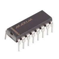
DG441DJ+ Maxim Integrated Products, DG441DJ+ Datasheet - Page 4

DG441DJ+
Manufacturer Part Number
DG441DJ+
Description
IC SWITCH QUAD SPST 16DIP
Manufacturer
Maxim Integrated Products
Datasheet
1.DG441DY.pdf
(9 pages)
Specifications of DG441DJ+
Function
Switch
Circuit
4 x SPST - NC
On-state Resistance
85 Ohm
Voltage Supply Source
Single, Dual Supply
Voltage - Supply, Single/dual (±)
10 V ~ 30 V, ±4.5 V ~ 20 V
Operating Temperature
-40°C ~ 85°C
Mounting Type
Through Hole
Package / Case
16-DIP (0.300", 7.62mm)
Number Of Switches
Quad
Switch Configuration
SPST
On Resistance (max)
100 Ohms
On Time (max)
250 ns
Off Time (max)
170 ns
Off Isolation (typ)
60 dB
Supply Voltage (max)
30 V
Supply Voltage (min)
10 V
Supply Current
15 uA
Maximum Power Dissipation
842 mW
Maximum Operating Temperature
+ 85 C
Mounting Style
Through Hole
Minimum Operating Temperature
- 40 C
Off State Leakage Current (max)
20 nA
Lead Free Status / RoHS Status
Lead free / RoHS Compliant
ELECTRICAL CHARACTERISTICS—Single Supply
(V+ = 12V, V- = 0V, V
Improved, Quad, SPST Analog Switches
Note 2: Typical values are for design aid only, are not guaranteed, and are not subject to production testing. The algebraic con-
Note 3: Guaranteed by design.
Note 4: On-resistance match between channels and flatness is guaranteed only with bipolar-supply operation. Flatness is defined
Note 5: Leakage parameters I
Note 6: Off-Isolation Rejection Ratio = 20log (V
Note 7: Between any two switches.
4
(T
__________________________________________Typical Operating Characteristics
SWITCH
Analog Signal Range
Drain-Source
On-Resistance
SUPPLY
Power-Supply Range
Positive Supply Current
Negative Supply Current
Ground Current
DYNAMIC
Turn-On Time
Turn-Off Time
Charge Injection (Note 3)
A
= +25°C, unless otherwise noted.)
_______________________________________________________________________________________
-1
-2
4
3
2
1
0
-15
PARAMETER
vention, where the most negative value is a minimum and the most positive value a maximum, is used in this data sheet.
as the difference between the maximum and the minimum value of on-resistance as measured at the extremes of the speci-
fied analog range.
by correlation at +25°C.
V+ = 15V
V- = -15V
T
A
-10
= +125°C
ON-LEAKAGE CURRENTS
-5
V S , V D (V)
GND
0
= 0V, V
SYMBOL
V
5
r
ANALOG
T
DS(ON)
S(OFF)
I
A
t
GND
t
V+
OFF
ON
= +85°C
I+
Q
I-
INH
10
= 2.4V, V
, I
D(OFF)
15
(Note 3)
V+ = 10.8V, V
I
All channels on or off, V
All channels on or off,
V
All channels on or off, V
V
V
C
S
IN
S
S
L
= 1.0mA
= 8V, Figure 2
= 8V, Figure 2
= 1nF, V
= 0V or 5V
, and I
INL
D
/V
= 0.8V, T
-1
2
1
0
S
-15
D(ON)
), V
GEN
V+ = 15V
V- = -15V
D
T
D
A
-10
= 3V, 8V,
= 0V
= +85°C
are 100% tested at the maximum rated hot temperature and guaranteed
= output, V
OFF-LEAKAGE CURRENTS
A
CONDITIONS
= T
-5
MIN
IN
IN
V S , V D (V)
= 0V or 5V
= 0V or 5V
to T
0
S
= input to off switch.
MAX
T
T
T
T
T
T
T
5
A
A
A
A
A
A
A
, unless otherwise noted.)
T
A
= +25°C
= T
= +25°C
= T
= +25°C
= +25°C
= +25°C
= +125°C
10
MIN
MIN
to T
to T
15
MAX
MAX
3.5
3.0
2.5
2.0
1.5
0.5
0
-100
±5
MIN
10
-1
-5
0
SWITCHING THRESHOLD vs.
BIPOLAR SUPPLY VOLTAGE
BIPOLAR SUPPLY VOLTAGE (V)
(Note 2)
-0.0001
TYP
100
300
-15
±10
15
60
5
MAX
MIN
MAX
160
200
100
400
200
12
30
10
1
5
±15
UNITS
µA
µA
µA
pC
ns
ns
Ω
V
V
±20


