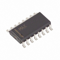
MAX9152ESE+T Maxim Integrated Products, MAX9152ESE+T Datasheet - Page 8

MAX9152ESE+T
Manufacturer Part Number
MAX9152ESE+T
Description
IC CROSSPOINT SWITCH 2X2 16SOIC
Manufacturer
Maxim Integrated Products
Datasheet
1.MAX9152EUE.pdf
(12 pages)
Specifications of MAX9152ESE+T
Function
Crosspoint Switch
Circuit
1 x 2:2
Voltage Supply Source
Single Supply
Voltage - Supply, Single/dual (±)
3 V ~ 3.6 V
Operating Temperature
-40°C ~ 85°C
Mounting Type
Surface Mount
Package / Case
16-SOIC (0.154", 3.90mm Width)
Lead Free Status / RoHS Status
Lead free / RoHS Compliant
800Mbps LVDS/LVPECL-to-LVDS 2 x 2
Crosspoint Switch
or EN1 low puts the corresponding driver output into a
high-impedance state (the differential output resistance
also becomes high impedance).
Figure 4. Output Active to High-Z and High-Z to Active Test
Circuit and Timing Diagram
Figure 5. Output Transition Time, Propagation Delay, and Output Channel-to-Channel Skew Test Circuit
8
V
V
V
V
OUT_
OUT_
OUT_
OUT_
GENERATOR
_______________________________________________________________________________________
+ WHEN V
- WHEN V
+ WHEN V
- WHEN V
PULSE
EN_
ID
ID
ID
ID
GENERATOR
= -100mV
= +100mV
= +100mV
= -100mV
IN_+
IN_-
PULSE
EN_
50Ω
t
t
1.5V
PHZ
PLZ
V
ID
50Ω
1/2 MAX9152
50%
50%
= (V
IN_+
50Ω
)–(V
IN_-
IN0+
IN0-
IN1+
)
IN1-
ENABLED
C
C
MAX9152
L
L
OUT_+
OUT_-
t
t
1.5V
PZH
PZL
R
R
L
L
/2
/2
50%
50%
+1.2V
3V
0
VOH
1.2V
1.2V
VOL
0
1
0
1
SEL0
SEL1
Unused differential inputs should be tied to ground and
V
ing due to noise. IN_+ should be pulled to V
10kΩ and IN_- should be pulled to GND with 10kΩ.
Devices can be cascaded to make larger switches.
Total propagation delay and total jitter should be con-
sidered to determine the maximum allowable switch
size. Three MAX9152s are needed to make a 2 input x
4 output crosspoint switch with two device propagation
delays. Seven MAX9152s make a 2 input x 8 output
crosspoint with three device delays.
The inputs accept PECL signals with the use of an
attenuation circuit, as shown in Figure 9.
Bypass V
mount ceramic 0.1µF and 0.001µF capacitors in paral-
Table 1. Input/Output Function Table
CC
SEL0
H
H
L
L
to prevent the high-speed input stage from switch-
CC
SEL1
to ground with high-frequency surface-
H
H
L
L
C
C
Applications Information
L
L
C
C
L
L
Unused Differential Inputs
OUT0
Power-Supply Bypassing
IN0
IN0
IN1
IN1
R
R
OUT1+
OUT0+
OUT1-
Accepting PECL Inputs
L
OUT0-
L
Expanding the Number
of LVDS Output Ports
OUT1
IN0
IN1
IN0
IN1
1:2 splitter
1:2 splitter
Repeater
MODE
Switch
CC
with


