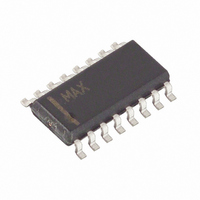
MAX9152ESE+T Maxim Integrated Products, MAX9152ESE+T Datasheet - Page 7

MAX9152ESE+T
Manufacturer Part Number
MAX9152ESE+T
Description
IC CROSSPOINT SWITCH 2X2 16SOIC
Manufacturer
Maxim Integrated Products
Datasheet
1.MAX9152EUE.pdf
(12 pages)
Specifications of MAX9152ESE+T
Function
Crosspoint Switch
Circuit
1 x 2:2
Voltage Supply Source
Single Supply
Voltage - Supply, Single/dual (±)
3 V ~ 3.6 V
Operating Temperature
-40°C ~ 85°C
Mounting Type
Surface Mount
Package / Case
16-SOIC (0.154", 3.90mm Width)
Lead Free Status / RoHS Status
Lead free / RoHS Compliant
The differential inputs of the MAX9152 do not have
internal fail-safe biasing. If fail-safe biasing is required,
it can be implemented with external large-value resis-
tors. IN_+ should be pulled up to V
IN_ should be pulled down to GND with 10kΩ. The volt-
age-divider formed by the 10kΩ resistors and the 100Ω
termination resistor (across IN_+ and IN_-) provides a
slight positive differential bias and sets a high state at
the device output when inputs are undriven.
The MAX9152 has a selectable differential output resis-
tance to reduce reflections from impedance discontinu-
ities in the interconnect. Reflections are reduced,
Figure 2. Input to Rising Edge Select Setup, Hold, and Mux Switch Timing Diagram
Figure 3. Input to Falling Edge Select Setup, Hold, and Mux Switch Timing Diagram
OUT_+
OUT_-
OUT_+
OUT_-
SEL_
IN0+
IN1+
IN0-
IN1-
SEL_
EN0 = EN1 = HIGH
IN0+
IN1+
V
IN0-
IN1-
EN0 = EN1 = HIGH
V
ID
ID
= (V
= (V
_______________________________________________________________________________________
IN_+
IN_+
) − (V
) − (V
IN_-
IN_-
800Mbps LVDS/LVPECL-to-LVDS 2 x 2
)
)
Output Resistance
V
V
V
V
ID
ID
ID
ID
= 0
= 0
= 0
= 0
t
Input Fail-Safe
CC
SET
t
SET
with 10kΩ and
1.5V
1.5V
t
HOLD
t
HOLD
t
SWITCH
t
SWITCH
IN0
IN1
compared to a high-impedance output. A termination
resistor at the receiver is still required and is the primary
termination for the interconnect. Select the output resis-
tance that best matches the differential characteristic
impedance of the interconnect used.
The SEL0 and SEL1 logic inputs allow the device to be
configured as a high-speed differential crosspoint, 2:1
mux, 1:2 demux, dual repeater, or 1:2 splitter (Figure
8). See
The EN0 and EN1 logic inputs enable and disable dri-
ver outputs OUT0 and OUT1. Setting EN0 or EN1 high
enables the corresponding driver output. Setting EN0
Table 1 for mode selection settings.
Crosspoint Switch
IN1
IN0
Enable Function
Select Function
7


