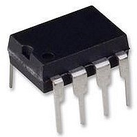
A25L010-F AMIC, A25L010-F Datasheet - Page 23

A25L010-F
Manufacturer Part Number
A25L010-F
Description
58T1296
Manufacturer
AMIC
Datasheet
1.A25L010-F.pdf
(44 pages)
Specifications of A25L010-F
Memory Type
Flash
Memory Size
1Mbit
Memory Configuration
1M X 1
Interface Type
Serial, SPI
Clock Frequency
100MHz
Supply Voltage Range
2.7V To 3.6V
Memory Case Style
DIP
No. Of Pins
8
Rohs Compliant
Yes
Chip Erase (CE)
The Chip Erase (CE) instruction sets all bits to 1 (FFh). Before
it can be accepted, a Write Enable (WREN) instruction must
previously have been executed. After the Write Enable
(WREN) instruction has been decoded, the device sets the
Write Enable Latch (WEL).
The Chip Erase (CE) instruction is entered by driving Chip
Select (
Data Input (DIO). Chip Select (
entire duration of the sequence.
The instruction sequence is shown in Figure 15. Chip Select
(
code has been latched in, otherwise the Bulk Erase instruction
Figure 15. Chip Erase (CE) Instruction Sequence
(December, 2010, Version 1.6)
S
) must be driven High after the eighth bit of the instruction
S
) Low, followed by the instruction code on Serial
DIO
C
S
S
) must be driven Low for the
0
1 2 3
Instruction
22
4 5 6 7
is not executed. As soon as Chip Select (
the self-timed Chip Erase cycle (whose duration is t
initiated. While the Chip Erase cycle is in progress, the Status
Register may be read to check the value of the Write In
Progress (WIP) bit. The Write In Progress (WIP) bit is 1 during
the self-timed Chip Erase cycle, and is 0 when it is completed.
At some unspecified time before the cycle is completed, the
Write Enable Latch (WEL) bit is reset.
The Chip Erase (CE) instruction is executed only if all Block
Protect (BP2, BP1, BP0) bits are 0. The Chip Erase (CE)
instruction is ignored if one, or more, blocks are protected.
A25L020/A25L010/A25L512 Series
AMIC Technology Corp.
S
) is driven High,
CE
) is


