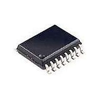
I74F3037D NXP Semiconductors, I74F3037D Datasheet - Page 4

I74F3037D
Manufacturer Part Number
I74F3037D
Description
Gates (AND / NAND / OR / NOR) QUAD 2-IN NAND TRN LN DRV IND
Manufacturer
NXP Semiconductors
Datasheet
1.N74F3037N602.pdf
(8 pages)
Specifications of I74F3037D
Product
NAND
Logic Family
F
Number Of Gates
4
Number Of Lines (input / Output)
2 / 1
High Level Output Current
- 67 mA
Low Level Output Current
160 mA
Propagation Delay Time
5 ns
Supply Voltage (max)
5.5 V
Supply Voltage (min)
4.5 V
Maximum Operating Temperature
+ 85 C
Mounting Style
SMD/SMT
Package / Case
SOT-162
Minimum Operating Temperature
- 40 C
Lead Free Status / Rohs Status
Details
Other names
I74F3037D,512
1. For conditions shown as MIN or MAX, use the appropriate value specified under recommended operating conditions for the applicable type.
2. All typical values are at V
3. I
4. I
5. I
Philips Semiconductors
RECOMMENDED OPERATING CONDITIONS
DC ELECTRICAL CHARACTERISTICS
(Over recommended operating free-air temperature range unless otherwise noted.)
Notes to DC electrical characteristics
AC ELECTRICAL CHARACTERISTICS
February 9, 1990
V
V
V
I
I
I
T
SYMBOL
Ik
OH
OL
SYMBOL
V
V
V
I
I
I
I
I
SYMBOL
t
t
amb
CC
IH
IL
I
IH
IL
O
CC
PLH
PHL
Quad 2-input NAND 30 driver
OH
OL
IK
UNIT
OH1
OL1
O
is tested under conditions that produce current approximately one half of the true short–circuit current (I
is the current necessary to guarantee the high to low transition in a 30 ohm transmission line on the incident wave.
is the current necessary to guarantee the low to high transition in a 30 ohm transmission line on the incident wave.
Supply voltage
High–level input voltage
Low–level input voltage
Input clamp current
High–level output current
Low–level output current
Operating free air temperature range
High–level output voltage
Low–level output voltage
Input clamp voltage
Input current at maximum input voltage
High–level input current
Low–level input current
Output current
Supply current (total)
Propagation delay
Dna, Dnb to Qn
PARAMETER
PARAMETER
5
CC
= 5V, T
amb
= 25 C.
PARAMETER
CONDITION
Waveform 1
TEST
I
I
CCH
CCL
V
V
V
V
MAX,
V
V
V
V
V
V
V
CC
IL
IH
CC
IH
CC
CC
CC
CC
CC
CC
MIN
1.0
1.0
= MAX,
= MIN
= MIN
= MIN,
= MIN, V
= MIN, I
= MAX, V
= MAX, V
= MAX, V
= MAX, V
= MAX
T
V
amb
C
R
CC
L
L
= 50pF,
= 500
TYP
= +5.0V
2.0
2.0
= +25 C
Commercial range
I
Industrial range
4
IL
= I
I
I
I
O
= 7.0V
= 2.7V
= 0.5V
=
= 2.25V
IK
MAX
CONDITIONS
5.0
4.5
TEST
I
I
T
OH
OL
V
amb
–67mA
160mA
CC
MIN
I
1.0
1.0
I
= 100mA
= –45mA
OH1
OL1
C
R
= 0 C to +70 C
= +5.0V
1
L
L
=
=
= 50pF,
LIMITS
= 500
3
4
MIN
–40
4.5
2.4
0
MAX
5.5
5.0
10%
10%V
10%V
10%V
5%V
5%V
CC
CC
CC
CC
CC
LIMITS
OS
NOM
T
5.0
amb
).
V
MIN
CC
-100
MIN
1.0
1.0
2.5
2.7
2.0
=–40 C to +85 C
C
R
= +5.0V
L
L
= 50pF,
= 500
LIMITS
TYP
-0.73
0.30
0.30
6.0
30
Product specification
MAX
–18
–67
160
5.5
0.8
+70
+85
74F3037
2
MAX
5.5
5.0
10%
MAX
-200
0.50
0.50
-1.2
-0.6
100
9.0
20
40
–40 to
+85 C
T
UNIT
UNIT
mA
mA
mA
A
mA
mA
mA
mA
ns
V
V
V
C
C
V
V
V
V
V
V
=
A
A


