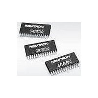
FM18L08-70-S Ramtron, FM18L08-70-S Datasheet - Page 7

FM18L08-70-S
Manufacturer Part Number
FM18L08-70-S
Description
F-RAM 256K (32Kx8) 70ns 3V
Manufacturer
Ramtron
Datasheet
1.FM18L08-70-TG.pdf
(13 pages)
Specifications of FM18L08-70-S
Memory Size
256 KB
Organization
32 K x 8
Interface
Parallel
Access Time
70 ns
Operating Supply Voltage
3 V to 3.6 V
Operating Temperature Range
- 40 C to + 85 C
Package / Case
SOIC-28
Mounting Style
SMD/SMT
Lead Free Status / Rohs Status
No
Available stocks
Company
Part Number
Manufacturer
Quantity
Price
Company:
Part Number:
FM18L08-70-S
Manufacturer:
RAMTRON
Quantity:
5 510
Part Number:
FM18L08-70-S
Manufacturer:
RAMTRON
Quantity:
20 000
Company:
Part Number:
FM18L08-70-SG
Manufacturer:
RAMTRON
Quantity:
15 040
Company:
Part Number:
FM18L08-70-SG
Manufacturer:
RAMRON
Quantity:
77
Part Number:
FM18L08-70-SG
Manufacturer:
RAMTRON
Quantity:
20 000
Company:
Part Number:
FM18L08-70-SGTR
Manufacturer:
ON
Quantity:
2 000
Part Number:
FM18L08-70-SGTR
Manufacturer:
RAMTRON
Quantity:
20 000
Read Cycle AC Parameters
Write Cycle AC Parameters
Notes
1
2
Data Retention
Power Cycle Timing
Capacitance
Rev. 3.5
Sept. 2009
Symbol
t
t
t
t
t
t
t
t
t
Symbol
t
t
t
t
t
t
t
t
t
t
t
t
t
t
Data Retention
t
t
C
C
CE
CA
RC
PC
AS
AH
OE
HZ
OHZ
CA
CW
WC
PC
AS
AH
WP
DS
DH
WZ
WX
HZ
WS
WH
PU
PD
Symbol
Symbol
I/O
IN
This parameter is periodically sampled and not 100% tested.
The relationship between /CE and /WE determines if a /CE- or /WE-controlled write occurs. There is no timing
specification associated with this relationship.
V
Last Access Complete to V
Input/Output Capacitance (DQ)
Input Capacitance
(T
Parameter
Chip Enable Access Time ( to data valid)
Chip Enable Active Time
Read Cycle Time
Precharge Time
Address Setup Time
Address Hold Time
Output Enable Access Time
Chip Enable to Output High-Z
Output Enable to Output High-Z
Parameter
Chip Enable Active Time
Chip Enable to Write High
Write Cycle Time
Precharge Time
Address Setup Time
Address Hold Time
Write Enable Pulse Width
Data Setup
Data Hold
Write Enable Low to Output High Z
Write Enable High to Output Driven
Chip Enable to Output High-Z
Write Setup
Write Hold
Parameter
DD
(V
A
= 25 C , f=1 MHz, V
DD
(min.) to First Access Start
= 3.0V to 3.65V)
(T
A
= -40 C to + 85 C, V
Parameter
Parameter
(T
(T
A
A
= -40 C to + 85 C, V
= -40 C to + 85 C, V
DD
= 3.3V)
DD
(min.)
DD
= 3.0V to 3.65V)
Min
45
DD
DD
Min
Max
= 3.0V to 3.65V)
0
= 3.0V to 3.65V)
1
8
6
Years
Units
Units
Units
Min
Min
140
140
pF
pF
70
70
15
70
70
70
15
40
40
10
0
0
0
0
0
S
S
Notes
Notes
Notes
1
2,000
2,000
Max
Max
70
10
15
15
15
15
Units
Units
ns
ns
ns
ns
ns
ns
ns
ns
ns
ns
ns
ns
ns
ns
ns
ns
ns
ns
ns
ns
ns
ns
ns
FM18L08
Notes
Notes
1
1
1
1
1
2
2
7 of 13


