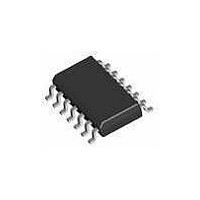
N74F74D NXP Semiconductors, N74F74D Datasheet - Page 3

N74F74D
Manufacturer Part Number
N74F74D
Description
Flip Flops DUAL D F/F EDGE TRIG
Manufacturer
NXP Semiconductors
Datasheet
1.N74F74N602.pdf
(8 pages)
Specifications of N74F74D
Number Of Circuits
2
Logic Family
N74F
Logic Type
D-Type Flip-Flop
Polarity
Inverting/Non-Inverting
Input Type
Single-Ended
Propagation Delay Time
8.5 ns
High Level Output Current
- 1 mA
Supply Voltage (max)
5.5 V
Maximum Operating Temperature
+ 85 C
Mounting Style
SMD/SMT
Package / Case
SOT-108
Minimum Operating Temperature
- 40 C
Supply Voltage (min)
4.5 V
Lead Free Status / Rohs Status
Details
Other names
N74F74D,602
Available stocks
Company
Part Number
Manufacturer
Quantity
Price
Company:
Part Number:
N74F74D
Manufacturer:
PHILIPS
Quantity:
1 376
Part Number:
N74F74D
Manufacturer:
PHILIPS/飞利浦
Quantity:
20 000
Philips Semiconductors
LOGIC DIAGRAM
ABSOLUTE MAXIMUM RATINGS
(Operation beyond the limit set forth in this table may impair the useful life of the device.
Unless otherwise noted these limits are over the operating free air temperature range.)
RECOMMENDED OPERATING CONDITIONS
1996 Mar 12
V
V
I
V
I
T
T
T
V
V
V
I
I
I
T
T
V
GND = Pin 7
IN
OUT
Ik
OH
OL
SYMBOL
SYMBOL
SYMBOL
amb
stg
amb
CC
CC
IN
OUT
CC
IH
IL
Dual D-type flip-flop
b
= Pin 14
SD
RD
CP
D
4, 10
1, 13
2, 12
3, 11
Supply voltage
Input voltage
Input current
Voltage applied to output in high output state
Current applied to output in low output state
Operating free air temperature range
Operating free air temperature range
Storage temperature range
Supply voltage
High-level input voltage
Low-level input voltage
Input clamp current
High-level output current
Low-level output current
Operating free air temperature range
O erating free air tem erature range
PARAMETER
PARAMETER
PARAMETER
SF00048
5, 9
6, 8
Q
Q
Commercial range
Industrial range
3
FUNCTION TABLE
NOTES:
H = High voltage level
h = High voltage level one setup time prior to low-to-high clock
L = Low voltage level
l
NC= No change from the previous setup
X = Don’t care
*
SD
H
H
H
H
L
L
transition
= Low voltage level one setup time prior to low-to-high clock
transition
= Low-to-high clock transition
= Not low-to-high clock transition
= This setup is unstable and will change when either set or reset
return to the high level.
Commercial range
Industrial range
RD
H
H
H
H
L
L
INPUTS
CP
X
X
X
MIN
–40
4.5
2.0
0
D
X
X
X
X
h
l
LIMITS
NOM
NC
OUTPUTS
Q
H
H
H
5.0
L
L
–0.5 to +7.0
–65 to +150
–0.5 to V
–0.5 to +7.0
–40 to +85
–30 to +5
RATING
0 to +70
NC
40
Q
H
H
H
L
L
CC
MAX
–18
+70
+85
5.5
0.8
Asynchronous set
Asynchronous reset
Undetermined*
Load ”1”
Load ”0”
Hold
–1
20
Product specification
OPERATING
MODE
74F74
UNIT
UNIT
UNIT
mA
mA
mA
mA
mA
V
V
V
V
V
V
C
C
C
C
C


