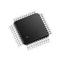
SC28L92A1B NXP Semiconductors, SC28L92A1B Datasheet - Page 56

SC28L92A1B
Manufacturer Part Number
SC28L92A1B
Description
UART Interface IC UART DUAL W/FIFO
Manufacturer
NXP Semiconductors
Type
Dual UARTr
Datasheet
1.SC28L92A1B557.pdf
(73 pages)
Specifications of SC28L92A1B
Number Of Channels
2
Data Rate
230.4 Kbps
Supply Voltage (max)
5 V
Supply Voltage (min)
3.3 V
Supply Current
25 mA
Maximum Operating Temperature
+ 85 C
Minimum Operating Temperature
- 40 C
Package / Case
PQFP-44
Description/function
Single-chip CMOS-LSI communications device
Mounting Style
SMD/SMT
Operating Supply Voltage
3.3 V, 5 V
Lead Free Status / Rohs Status
Details
Other names
SC28L92A1B,557
Available stocks
Company
Part Number
Manufacturer
Quantity
Price
Part Number:
SC28L92A1B
Manufacturer:
PHILIPS/飞利浦
Quantity:
20 000
Company:
Part Number:
SC28L92A1B,528
Manufacturer:
NXP Semiconductors
Quantity:
10 000
Company:
Part Number:
SC28L92A1B,551
Manufacturer:
NXP Semiconductors
Quantity:
10 000
Company:
Part Number:
SC28L92A1B,557
Manufacturer:
NXP Semiconductors
Quantity:
10 000
Company:
Part Number:
SC28L92A1BS,528
Manufacturer:
NXP Semiconductors
Quantity:
10 000
Company:
Part Number:
SC28L92A1BS,551
Manufacturer:
NXP Semiconductors
Quantity:
10 000
NXP Semiconductors
[7]
Table 68.
V
SC28L92_7
Product data sheet
Symbol
Reset timing (see
t
Bus timing
t
t
t
t
t
t
t
t
t
t
t
t
Port timing
t
t
t
Interrupt timing (see
t
RES
AS
AH
CS
CH
RW
DD
DA
DF
DI
DS
DH
RWD
PS
PH
PD
IR
CC
Minimum DACKN time is ((t
cycles, the 80xxx bus timing may be used while in the 68xxx mode. It is not necessary to wait for DACKN to insure the proper operation
of the SC26C92. In all cases the data will be written to the SC28L92 on the falling edge of DACKN or the rise of CEN. The fall of CEN
initializes the bus cycle. The rise of CEN ends the bus cycle. DACKN LOW or CEN HIGH completes the write cycle.
= 3.3 V
Parameter
reset pulse width
A0 to A3 set-up time to RDN, WRN LOW
A0 to A3 hold time from RDN, WRN LOW
CEN set-up time to RDN, WRN LOW
CEN hold time from RDN, WRN LOW
WRN, RDN pulse width (LOW time)
data valid after RDN LOW
RDN LOW to data bus active
data bus floating after RDN or CEN HIGH
RDN or CEN HIGH to data bus invalid
data bus set-up time before WRN or CEN
HIGH (write cycle)
data hold time after WRN HIGH
HIGH time between read and/or write
cycles
port in set-up time before RDN LOW
(Read IP ports cycle)
port in hold time after RDN HIGH
OP port valid after WRN or CEN HIGH
(OPR write cycle)
INTRN (or OP3 to OP7 when used as
interrupts)
Dynamic characteristics, 3.3 V operation
[2]
[2]
10 %, T
(see
(see
Figure
Figure
Figure
amb
Figure
= 40 C to +85 C, unless otherwise specified.
10)
11)
15)
DCR
16)
or t
DCW
) t
CSC
+ 2 X1 edges + rise time over 5 ns). Two X1 edges is 273 ns at 3.6864 MHz. For faster bus
Rev. 07 — 19 December 2007
3.3 V/5.0 V Dual Universal Asynchronous Receiver/Transmitter
[1]
Conditions
125 pF load; see
for smaller loads
read Rx FIFO
(RxRDY/FFULL interrupt)
write Tx FIFO (TxRDY
interrupt)
reset command (delta
break change interrupt)
stop C/T command
(counter/timer interrupt
read IPCR (delta input port
change interrupt)
write IMR (clear of change
interrupt mask bit(s))
Figure 9
[2][4]
[3]
[4]
Min
100
10
33
0
0
20
-
0
-
0
43
0
27
0
0
-
-
-
-
-
-
-
Typ
20
6
16
-
-
10
46
-
15
-
20
10
50
40
40
40
40
40
40
15
20
20
SC28L92
© NXP B.V. 2007. All rights reserved.
Max
-
-
-
-
-
-
75
-
20
-
-
-
-
-
-
75
79
79
79
79
79
79
56 of 73
Unit
ns
ns
ns
ns
ns
ns
ns
ns
ns
ns
ns
ns
ns
ns
ns
ns
ns
ns
ns
ns
ns
ns


