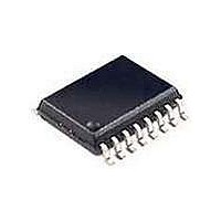
74LV4053PW NXP Semiconductors, 74LV4053PW Datasheet - Page 5

74LV4053PW
Manufacturer Part Number
74LV4053PW
Description
Multiplexer Switch ICs TRIPLE 2-CHANNEL MUX/DMUX
Manufacturer
NXP Semiconductors
Type
Analog Multiplexerr
Datasheet
1.74LV4053N112.pdf
(26 pages)
Specifications of 74LV4053PW
Number Of Channels
3 Channel
On Resistance (max)
180 Ohms
Propagation Delay Time
25 ns, 9 ns, 6 ns, 5 ns, 4 ns, 3 ns
On Time (max)
125 ns
Off Time (max)
95 ns
Supply Voltage (max)
6 V
Supply Voltage (min)
1 V
Maximum Power Dissipation
400 mW
Maximum Operating Temperature
+ 125 C
Minimum Operating Temperature
- 40 C
Package / Case
TSSOP-16
Mounting Style
SMD/SMT
Number Of Lines (input / Output)
6 / 3
Package
16TSSOP
Maximum On Resistance
435@2V Ohm
Maximum Propagation Delay Bus To Bus
25(Typ)@1.2V|9(Typ)@2V|6(Typ)@2.7V|5(Typ)@3.3V|4(Typ)@4.5V|3(Typ)@6V ns
Maximum Low Level Output Current
25 mA
Multiplexer Architecture
2:1
Maximum Turn-off Time
95(Typ)@1.2V ns
Maximum Turn-on Time
125(Typ)@1.2V ns
Power Supply Type
Single
Lead Free Status / Rohs Status
Details
Other names
74LV4053PW,112
Available stocks
Company
Part Number
Manufacturer
Quantity
Price
Company:
Part Number:
74LV4053PW
Manufacturer:
MOT
Quantity:
5 510
NXP Semiconductors
6. Functional description
Table 3.
[1]
7. Limiting values
Table 4.
In accordance with the Absolute Maximum Rating System (IEC 60134). Voltages are referenced to V
[1]
[2]
[3]
74LV4053_4
Product data sheet
Inputs
E
L
L
H
Symbol
V
I
I
I
T
P
IK
SK
SW
stg
CC
tot
H = HIGH voltage level; L = LOW voltage level; X = don’t care.
To avoid drawing V
switch must not exceed 0.4 V. If the switch current flows into terminal nZ, no V
there is no limit for the voltage drop across the switch, but the voltages at nYn and nZ may not exceed V
The minimum input voltage rating may be exceeded if the input current rating is observed.
For DIP16 packages: above 70 C the value of P
For SO16 packages: above 70 C the value of P
For SSOP16 and TSSOP16 packages: above 60 C the value of P
For DHVQFN16 packages: above 60 C the value of P
Function table
Limiting values
Parameter
supply voltage
input clamping current
switch clamping current
switch current
storage temperature
total power dissipation
CC
current out of terminal nZ, when switch current flows into terminals nYn, the voltage drop across the bidirectional
[1]
Sn
L
H
X
Conditions
V
V
V
source or sink current
T
amb
I
SW
SW
DIP16 package
SO16 package
TSSOP16 package
DHVQFN16 package
< 0.5 V or V
< 0.5 V or V
> 0.5 V or V
tot
= 40 C to +125 C
tot
derates linearly with 8 mW/K.
derates linearly with 12 mW/K.
Rev. 04 — 10 August 2009
tot
derates linearly with 4.5 mW/K.
I
> V
SW
SW
CC
tot
< V
> V
derates linearly with 5.5 mW/K.
+ 0.5 V
CC
CC
Triple single-pole double-throw analog switch
+ 0.5 V;
+ 0.5 V
CC
current will flow out of terminals nYn, and in this case
[1]
[2]
[2]
[2]
[3]
Channel on
nY0 to nZ
nY1 to nZ
switches off
Min
-
-
-
-
-
-
-
0.5
65
CC
or V
Max
+7.0
+150
750
500
500
500
SS
20
20
25
74LV4053
EE
= 0 V (ground).
© NXP B.V. 2009. All rights reserved.
.
Unit
V
mA
mA
mA
mW
mW
mW
mW
C
5 of 26


