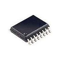
74LV4053PW NXP Semiconductors, 74LV4053PW Datasheet - Page 12

74LV4053PW
Manufacturer Part Number
74LV4053PW
Description
Multiplexer Switch ICs TRIPLE 2-CHANNEL MUX/DMUX
Manufacturer
NXP Semiconductors
Type
Analog Multiplexerr
Datasheet
1.74LV4053N112.pdf
(26 pages)
Specifications of 74LV4053PW
Number Of Channels
3 Channel
On Resistance (max)
180 Ohms
Propagation Delay Time
25 ns, 9 ns, 6 ns, 5 ns, 4 ns, 3 ns
On Time (max)
125 ns
Off Time (max)
95 ns
Supply Voltage (max)
6 V
Supply Voltage (min)
1 V
Maximum Power Dissipation
400 mW
Maximum Operating Temperature
+ 125 C
Minimum Operating Temperature
- 40 C
Package / Case
TSSOP-16
Mounting Style
SMD/SMT
Number Of Lines (input / Output)
6 / 3
Package
16TSSOP
Maximum On Resistance
435@2V Ohm
Maximum Propagation Delay Bus To Bus
25(Typ)@1.2V|9(Typ)@2V|6(Typ)@2.7V|5(Typ)@3.3V|4(Typ)@4.5V|3(Typ)@6V ns
Maximum Low Level Output Current
25 mA
Multiplexer Architecture
2:1
Maximum Turn-off Time
95(Typ)@1.2V ns
Maximum Turn-on Time
125(Typ)@1.2V ns
Power Supply Type
Single
Lead Free Status / Rohs Status
Details
Other names
74LV4053PW,112
Available stocks
Company
Part Number
Manufacturer
Quantity
Price
Company:
Part Number:
74LV4053PW
Manufacturer:
MOT
Quantity:
5 510
NXP Semiconductors
Table 8.
Voltages are referenced to GND (ground = 0 V). For test circuit see
[1]
[2]
[3]
[4]
74LV4053_4
Product data sheet
Symbol Parameter
t
C
dis
PD
All typical values are measured at T
t
t
t
Typical values are measured at nominal supply voltage (V
C
P
f
C
C
V
N = number of inputs switching
pd
en
dis
i
(C
D
CC
PD
= input frequency in MHz, f
L
SW
is the same as t
is the same as t
= output load capacitance in pF
is the same as t
= C
L
is used to determine the dynamic power dissipation (P
= supply voltage in Volts
= maximum switch capacitance in pF;
disable time
power dissipation
capacitance
PD
V
Dynamic characteristics
CC
2
V
CC
f
o
2
) = sum of the outputs.
PLH
PZL
f
PLZ
i
and t
N + ((C
and t
and t
PZH
PHL
PHZ
o
Conditions
E to nYn, nZ; see
Sn to nYn, nZ; see
C
V
= output frequency in MHz
I
L
.
.
.
L
V
V
V
V
V
V
V
V
V
V
V
V
V
V
= GND to V
= 50 pF; f
+ C
CC
CC
CC
CC
CC
CC
CC
CC
CC
CC
CC
CC
CC
CC
amb
SW
= 1.2 V
= 2.0 V
= 2.7 V
= 3.0 V to 3.6 V; C
= 3.0 V to 3.6 V
= 4.5 V
= 6.0 V
= 1.2 V
= 2.0 V
= 2.7 V
= 3.0 V to 3.6 V; C
= 3.0 V to 3.6 V
= 4.5 V
= 6.0 V
…continued
)
= 25 C.
V
i
CC
= 1 MHz;
CC
2
Figure 14
f
o
Figure 14
Rev. 04 — 10 August 2009
) where:
L
L
CC
D
= 15 pF
= 15 pF
= 3.3 V).
in W).
[2]
[3]
[3]
[2]
[3]
[3]
[4]
Figure
Triple single-pole double-throw analog switch
Min
-
-
-
-
-
-
-
-
-
-
-
-
-
-
-
40 C to +85 C
15.
Typ
95
34
26
17
20
18
15
90
32
24
16
19
17
14
36
[1]
Max
61
46
37
32
25
59
44
36
31
24
-
-
-
-
-
Min
40 C to +125 C
-
-
-
-
-
-
-
-
-
-
-
-
-
-
-
74LV4053
© NXP B.V. 2009. All rights reserved.
Max
73
54
44
38
30
70
52
42
36
28
-
-
-
-
-
12 of 26
Unit
ns
ns
ns
ns
ns
ns
ns
ns
ns
ns
ns
ns
ns
ns
pF


