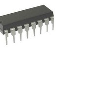
DG509AAK Vishay, DG509AAK Datasheet - Page 9

DG509AAK
Manufacturer Part Number
DG509AAK
Description
Multiplexer Switch ICs Dual 4:1 Multiplexer/MUX
Manufacturer
Vishay
Type
Analog Multiplexerr
Datasheet
1.DG509AAK883.pdf
(11 pages)
Specifications of DG509AAK
Number Of Channels
1 Channel
On Resistance (max)
400 Ohms
Propagation Delay Time
1000 ns
On Time (max)
1500 ns
Off Time (max)
1000 ns
Supply Voltage (max)
25 V
Supply Current
1.3 mA
Maximum Power Dissipation
900 mW
Maximum Operating Temperature
+ 125 C
Minimum Operating Temperature
- 55 C
Package / Case
CDIP-16
Mounting Style
Through Hole
Number Of Lines (input / Output)
8 / 2
Number Of Switches
2
Switch Current (typ)
1.3 mA at 15 V, - 0.7 mA at - 15 V
Lead Free Status / Rohs Status
In Transition
Available stocks
Company
Part Number
Manufacturer
Quantity
Price
Company:
Part Number:
DG509AAK
Manufacturer:
MAXIM
Quantity:
58
Overvoltage Protection
A very convenient form of overvoltage protection consists of
adding two small signal diodes (1N4148, 1N914 type) in series
with the supply pins (see Figure 11). This arrangement
effectively blocks the flow of reverse currents. It also floats the
supply pin above or below the normal V+ or V– value. In this
case the overvoltage signal actually becomes the power
supply of the IC. From the point of view of the chip, nothing has
changed, as long as the difference between V
doesn’t exceed +44 V. The addition of these diodes will reduce
the analog signal range to 1 V below V+ and 1 V above V–, but
it preserves the low channel resistance and low leakage
characteristics.
Document Number: 70067
S-00405—Rev. C, 21-Feb-00
V
S
R
g
= 50
Notes:
a.
b.
Positive Supply
S
A
A
A
1
0
1
2
GND
Application Hints are for DESIGN AID ONLY, not guaranteed and not subject to production testing.
Operation below
Voltage
FIGURE 8. Insertion Loss
V+
(V)
15
10
12
8
+15 V
b
EN
V+
Insertion Loss = 20 log
–15 V
V–
8 V is not recommended.
D
Negative Supply
Voltage
S
V–
(V)
–15
–12
–10
–8
and the V– rail
R
1 k
L
V
V
V
OUT
O
IN
Logic Input Voltage
V
INH(min)
Channel
Select
2.4/0.8
2.4/0.8
2.4/0.6
2.4/0.4
V
(V)
/V
IN
FIGURE 10. Overvoltage Protection Using Blocking Diodes
INL(max)
A
A
A
GND
2
1
0
V
g
V+ v V
FIGURE 9. Source Drain Capacitance
DG508A_MIL/509A_MIL
+15 V
Analog Voltage
EN
V+
g
v V–
V
–15 to 15
–12 to 12
–10 to 10
Range
S
S
–8 to 8
–15 V
X
(V)
or V
V–
S
S
D
1
8
www.vishay.com FaxBack 408-970-5600
D
+15 V
–15 V
Junction
Junction
Internal
Internal
V+
V–
DG508A_MIL
Vishay Siliconix
1N4148
1N4148
or Equivalent
Impedance
D
HP4192A
f = 1 MHz
Analyzer
Meter
5-9


