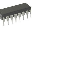
DG509AAK Vishay, DG509AAK Datasheet - Page 8

DG509AAK
Manufacturer Part Number
DG509AAK
Description
Multiplexer Switch ICs Dual 4:1 Multiplexer/MUX
Manufacturer
Vishay
Type
Analog Multiplexerr
Datasheet
1.DG509AAK883.pdf
(11 pages)
Specifications of DG509AAK
Number Of Channels
1 Channel
On Resistance (max)
400 Ohms
Propagation Delay Time
1000 ns
On Time (max)
1500 ns
Off Time (max)
1000 ns
Supply Voltage (max)
25 V
Supply Current
1.3 mA
Maximum Power Dissipation
900 mW
Maximum Operating Temperature
+ 125 C
Minimum Operating Temperature
- 55 C
Package / Case
CDIP-16
Mounting Style
Through Hole
Number Of Lines (input / Output)
8 / 2
Number Of Switches
2
Switch Current (typ)
1.3 mA at 15 V, - 0.7 mA at - 15 V
Lead Free Status / Rohs Status
In Transition
Available stocks
Company
Part Number
Manufacturer
Quantity
Price
Company:
Part Number:
DG509AAK
Manufacturer:
MAXIM
Quantity:
58
DG508A_MIL/509A_MIL
Vishay Siliconix
www.vishay.com FaxBack 408-970-5600
5-8
V
g
V
+2.4 V
S
R
g
= 50
R
g
50
Channel
V
Select
IN
EN
A
A
A
0
1
2
GND
S
S
A
A
A
X
8
0
1
2
DG508A_MIL
DG509A_MIL
GND
FIGURE 6. Off Isolation
+15 V
V+
All S and D
EN
S
A
A
A
EN
V+
X
0
1
2
GND
Off Isolation = 20 log
–15 V
+15 V
V–
D
–15 V
b
V–
, D
a
FIGURE 4. Break-Before-Make Interval
V+
300
D
+15 V
–15 V
+5 V
V–
FIGURE 5. Charge Injection
R
1 k
D
L
V
V
OUT
V
IN
35 pF
O
V
O
C
10 nF
L
V
O
R
g
Switch
Output
Logic
V
= 50
Input
Output
Switch
O
Logic
Input
V
S
3 V
0 V
error Q, when the channel turns off.
V
3 V
0 V
0 V
O
V
V
S
is the measured voltage due to charge transfer
OFF
IN
FIGURE 7. Crosstalk
S
S
S
A
A
A
1
X
8
0
1
2
GND
Q = C
50%
V+
EN
ON
Crosstalk = 20 log
L
x V
+15 V
S-00405—Rev. C, 21-Feb-00
–15 V
Document Number: 70067
80%
V–
O
t
OPEN
D
t
t
r
OFF
f
<20 ns
<20 ns
V
R
1 k
V
OUT
IN
L
V
O
V
O


