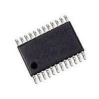
ADF7011BRUZ-REEL7 Analog Devices Inc, ADF7011BRUZ-REEL7 Datasheet - Page 4

ADF7011BRUZ-REEL7
Manufacturer Part Number
ADF7011BRUZ-REEL7
Description
Manufacturer
Analog Devices Inc
Datasheet
1.ADF7011BRUZ-REEL7.pdf
(24 pages)
Specifications of ADF7011BRUZ-REEL7
Operating Temperature (min)
-40C
Operating Temperature (max)
85C
Operating Temperature Classification
Industrial
Product Depth (mm)
4.4mm
Operating Supply Voltage (min)
2.3V
Operating Supply Voltage (typ)
2.5/3.3V
Operating Supply Voltage (max)
3.6V
Lead Free Status / Rohs Status
Compliant
ADF7011
TIMING CHARACTERISTICS
Parameter
t
t
t
t
t
t
Guaranteed by design but not production tested.
Specifications subject to change without notice.
ABSOLUTE MAXIMUM RATINGS
(T
V
CPV
Digital I/O Voltage to GND . . . . . . . –0.3 V to DV
Operating Temperature Range
Storage Temperature Range . . . . . . . . . . . . –65°C to +125°C
Maximum Junction Temperature . . . . . . . . . . . . . . . . . 125°C
TSSOP
Lead Temperature, Soldering
CAUTION
ESD (electrostatic discharge) sensitive device. Electrostatic charges as high as 4000 V readily
accumulate on the human body and test equipment and can discharge without detection. Although the
ADF7011 features proprietary ESD protection circuitry, permanent damage may occur on devices
subjected to high energy electrostatic discharges. Therefore, proper ESD precautions are recommended
to avoid performance degradation or loss of functionality.
1
2
3
4
5
6
DD
A
Industrial (B Version) . . . . . . . . . . . . . . . . –40°C to +85°C
Vapor Phase (60 sec) . . . . . . . . . . . . . . . . . . . . . . . . . 235°C
Infrared (15 sec) . . . . . . . . . . . . . . . . . . . . . . . . . . . . 240°C
= 25°C, unless otherwise noted.)
to GND
DD
DATA
CLOCK
LE
to GND . . . . . . . . . . . . . . . . . . . . . . . –0.3 V to + 7 V
JA
Thermal Impedance . . . . . . . . . . . . . . 150.4°C/W
3
. . . . . . . . . . . . . . . . . . . . . . . . . –0.3 V to + 7 V
DB23 (MSB)
Limit at
T
(B Version)
10
10
25
25
10
20
MIN
to T
MAX
t
1
1, 2
DB22
(V
Unit
ns min
ns min
ns min
ns min
ns min
ns min
DD
t
2
= 3 V
Figure 1. Timing Diagram
DD
10%; VGND = 0 V, T
+ 0.3 V
Test Conditions/Comments
DATA to CLOCK Setup Time
DATA to CLOCK Hold Time
CLOCK High Duration
CLOCK Low Duration
CLOCK to LE Setup Time
LE Pulsewidth
DB2
–4–
t
3
NOTES
1
2
3
Model
ADF7011BRU
ADF7011BRU-REEL
ADF7011BRU-REEL7
Stresses above those listed under Absolute Maximum Ratings may cause perma-
nent damage to the device. This is a stress rating only; functional operation of the
device at these or any other conditions above those listed in the operational
sections of this specification is not implied. Exposure to absolute maximum rating
conditions for extended periods may affect device reliability.
This device is a high performance RF integrated circuit with an ESD rating of
<1 kV and is ESD sensitive. Proper precautions should be taken for handling and
assembly.
GND = VCOGND = CPGND = RFGND = DGND = AGND = 0 V.
A
= 25 C, unless otherwise noted.)
t
4
(CONTROL BIT C2)
DB1
ORDERING GUIDE
Temperature
Range
–40ºC to +85ºC
–40ºC to +85ºC
–40ºC to +85ºC
(CONTROL BIT C1)
t
DB0 (LSB)
5
Package Option
RU-24 (TSSOP)
RU-24 (TSSOP)
RU-24 (TSSOP)
t
6
REV. 0


