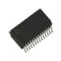
TDA5201XT Infineon Technologies, TDA5201XT Datasheet - Page 20

TDA5201XT
Manufacturer Part Number
TDA5201XT
Description
Manufacturer
Infineon Technologies
Datasheet
1.TDA5201XT.pdf
(38 pages)
Specifications of TDA5201XT
Operating Temperature (min)
-40C
Operating Temperature (max)
125C
Operating Temperature Classification
Automotive
Product Depth (mm)
4.4mm
Product Length (mm)
9.7mm
Operating Supply Voltage (min)
4.5V
Operating Supply Voltage (typ)
5V
Operating Supply Voltage (max)
5.5V
Lead Free Status / Rohs Status
Compliant
The calculation of the value of the necessary quartz load capacitance is shown in
frequency calculation is explained in
3.4.5
The Limiter is an AC coupled multistage amplifier with a cumulative gain of approximately 80 dB that has a
bandpass-characteristic centered around 10.7 MHz. It has an input impedance of 330 Ω to allow for easy
interfacing to a 10.7 MHz ceramic IF filter. The limiter circuit acts as a Receive Signal Strength Indicator (RSSI)
generator, which produces a DC voltage that is directly proportional to the input signal level as can be seen in
Figure
turn down the LNA gain by approximately 18 dB in case the input signal strength is too strong as described in
Chapter 3.4.1
3.4.6
The data filter comprises an OP-Amp with a bandwidth of 100 kHz used as a voltage follower and two 100 kΩ on-
chip resistors. Along with two external capacitors a 2
the capacitor values is described in
3.4.7
The data slicer is a fast comparator with a bandwidth of 100 kHz. This allows for a maximum receive data rate of
approximately 120 kBaud. The maximum achievable data rate also depends on the IF Filter bandwidth and the
local oscillator tolerance values. Both inputs are accessible. The output delivers a digital data signal (CMOS-like
levels) for the detector. The self-adjusting threshold on pin 20 is generated by RC-term or peak detector
depending on the baseband coding scheme. The data slicer threshold generation alternatives are described in
more detail in
3.4.8
The peak detector generates a DC voltage which is proportional to the peak value of the receive data signal. An
external RC network is necessary. The output can be used as an indicator for the signal strength and also as a
reference for the data slicer. The maximum output current is 500 µA.
3.4.9
A Bandgap Reference Circuit provides a temperature stable reference voltage for the device. A power down mode
is available to switch off all sub-circuits which is controlled by the PWDN pin (Pin 27) as shown in the following
table. The supply current drawn in this case is typically 50 nA.
Table 3
PDWN
Open or tied to ground
Tied to
Data Sheet
6. This signal is used to demodulate the ASK receive signal in the subsequent baseband circuitry and to
V
CC
Bandgap Reference Circuitry
Limiter
Data Filter
Data Slicer
Peak Detector
PDWN Pin Operating States
Chapter
and
Chapter
4.5.
4.1.
Chapter
Chapter
4.2.
4.4.
nd
order Sallen-Key low pass filter is formed. The selection of
20
Operating State
Power Down Mode
Receiver On
ASK Single Conversion Receiver
Revision 1.6, 2010-12-21
Functional Description
Chapter
4.3, the quartz
TDA 5201


