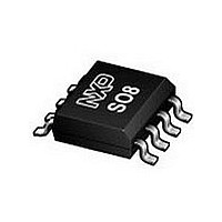
SA630D NXP Semiconductors, SA630D Datasheet - Page 4

SA630D
Manufacturer Part Number
SA630D
Description
Manufacturer
NXP Semiconductors
Datasheet
1.SA630D.pdf
(14 pages)
Specifications of SA630D
Number Of Switches
Single
Pin Count
8
Lead Free Status / Rohs Status
Not Compliant
Available stocks
Company
Part Number
Manufacturer
Quantity
Price
Company:
Part Number:
SA630D
Manufacturer:
NXPLIPS
Quantity:
5 510
Part Number:
SA630D
Manufacturer:
PHILIPS/飞利浦
Quantity:
20 000
Company:
Part Number:
SA630D/01
Manufacturer:
NXP
Quantity:
1 184
1. All measurements include the effects of the D package SA630 Evaluation Board (see Figure 4B). Measurement system impedance is 50 .
2. The placement of the AC bypass capacitor is critical to achieve these specifications. See the applications section for more details.
1. All measurements include the effects of the N package SA630 Evaluation Board (see Figure 4C). Measurement system impedance is 50 .
Philips Semiconductors
AC ELECTRICAL CHARACTERISTICS
V
NOTE:
AC ELECTRICAL CHARACTERISTICS
V
NOTE:
APPLICATIONS
The typical applications schematic and printed circuit board layout of
the SA630 evaluation board is shown in Figure 4. The layout of the
board is simple, but a few cautions need to be observed. The input
and output traces should be 50 . The placement of the AC bypass
capacitor is extremely critical if a symmetric isolation between the
two channels is desired. The trace from Pin 7 should be drawn back
towards the package and then be routed downwards. The capacitor
1997 Nov 07
SYMBOL
SYMBOL
DD
DD
S
S
S
S
S
S
Single pole double throw (SPDT) switch
21
21
11
11
P
21
21
t
IP
IP
NF
NF
= +5V, T
r
-1dB
= +5V, T
t
, S
, S
, S
, S
, t
, S
, S
D
3
2
f
12
12
22
22
12
12
Insertion loss (ON channel)
Isolation (OFF channel)
Return loss (ON channel)
Return loss (OFF channel)
Switching speed (on-off delay)
Switching speeds (on-off rise/fall time)
Switching transients
1dB gain compression
Third-order intermodulation intercept
Second-order intermodulation intercept
Noise figure (Z
Insertion loss (ON channel)
Isolation (OFF channel)
Noise figure (Z
A
A
= 25 C; unless otherwise stated.
= 25 C; all other characteristics similar to the D-Package, unless otherwise stated.
O
O
PARAMETER
PARAMETER
= 50 )
= 50 )
2
1
1
- D PACKAGE
- N PACKAGE
90%/10% to 10%/90% RF
50% TTL to 90/10% RF
4
TEST CONDITIONS
TEST CONDITIONS
should be placed straight down as close to the device as practical.
For better isolation between the two channels at higher frequencies,
it is also advisable to run the two output/input traces at an angle.
This also minimizes any inductive coupling between the two traces.
The power supply bypass capacitor should be placed close to the
device. Figure 10 shows the frequency response of the SA630.
The loss matching between the two channels is excellent to 1.2GHz
as shown in Figure 13.
DC - 100MHz
DC - 400MHz
DC - 400MHz
DC - 100MHz
DC - 1GHz
500MHz
900MHz
100MHz
500MHz
900MHz
900MHz
900MHz
100MHz
100MHz
100MHz
900MHz
500MHz
900MHz
100MHz
500MHz
900MHz
100MHz
900MHz
10MHz
10MHz
MIN
MIN
70
24
58
LIMITS
LIMITS
SA630
SA630
TYP
TYP
165
+18
+33
+52
1.4
1.0
2.0
1.4
2.5
1.0
2.5
80
60
50
30
20
12
17
13
20
68
50
37
15
1
2
5
1
Product specification
MAX
MAX
SA630
2.8
UNITS
UNITS
mV
dBm
dBm
dBm
dB
dB
dB
dB
dB
dB
dB
dB
ns
ns
P-P


