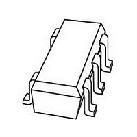
74HC1G08GW NXP Semiconductors, 74HC1G08GW Datasheet - Page 3

74HC1G08GW
Manufacturer Part Number
74HC1G08GW
Description
Manufacturer
NXP Semiconductors
Datasheet
1.74HC1G08GW.pdf
(11 pages)
Specifications of 74HC1G08GW
Logic Family
HC
Logical Function
AND
Number Of Elements
1
High Level Output Current
-2.6mA
Low Level Output Current
2.6mA
Operating Supply Voltage (typ)
5V
Operating Temp Range
-40C to 125C
Package Type
TSSOP
Number Of Outputs
1
Number Of Inputs
2-IN
Technology
CMOS
Mounting
Surface Mount
Pin Count
5
Operating Temperature Classification
Automotive
Quiescent Current
20uA
Operating Supply Voltage (max)
6V
Operating Supply Voltage (min)
2V
Lead Free Status / Rohs Status
Compliant
Available stocks
Company
Part Number
Manufacturer
Quantity
Price
Company:
Part Number:
74HC1G08GW
Manufacturer:
BCD
Quantity:
28
Part Number:
74HC1G08GW
Manufacturer:
NXP/恩智浦
Quantity:
20 000
Part Number:
74HC1G08GW,125
Manufacturer:
NEXPERIA/安世
Quantity:
20 000
NXP Semiconductors
7. Functional description
Table 4.
H = HIGH voltage level; L = LOW voltage level
8. Limiting values
Table 5.
In accordance with the Absolute Maximum Rating System (IEC 60134). Voltages are referenced to GND (ground = 0 V).
[1]
[2]
9. Recommended operating conditions
Table 6.
Voltages are referenced to GND (ground = 0 V).
74HC_HCT1G08_4
Product data sheet
Input
A
L
L
H
H
Symbol
V
I
I
I
I
I
T
P
Symbol Parameter
V
V
V
T
IK
OK
O
CC
GND
stg
amb
t/ V
CC
tot
CC
I
O
The input and output voltage ratings may be exceeded if the input and output current ratings are observed.
Above 55 C the value of P
supply voltage
input voltage
output voltage
ambient temperature
input transition rise
and fall rate
Function table
Limiting values
Recommended operating conditions
Parameter
supply voltage
input clamping current
output clamping current
output current
supply current
ground current
storage temperature
total power dissipation
tot
derates linearly with 2.5 mW/K.
Conditions
V
V
V
CC
CC
CC
= 2.0 V
= 4.5 V
= 6.0 V
B
L
H
L
H
Conditions
V
V
T
0.5 V < V
I
O
amb
< 0.5 V or V
< 0.5 V or V
= 40 C to +125 C
Rev. 04 — 17 July 2007
O
< V
I
CC
O
> V
> V
Min
+ 0.5 V
2.0
0
0
40
-
-
-
CC
CC
74HC1G08; 74HCT1G08
+ 0.5 V
74HC1G08
+ 0.5 V
Typ
+25
5.0
-
-
-
-
-
+125
Max
V
V
625
139
6.0
83
CC
CC
Output
Y
L
L
L
H
[2]
Min
4.5
Min
-
-
-
-
-
0
0
40
-
-
-
0.5
25
65
74HCT1G08
Typ
+25
5.0
-
-
-
-
-
Max
+7.0
25
-
+150
200
© NXP B.V. 2007. All rights reserved.
2-input AND gate
20
20
12.5
+125
Max
V
V
139
5.5
CC
CC
-
-
Unit
V
mA
mA
mA
mA
mA
mW
C
Unit
V
V
V
ns/V
ns/V
ns/V
C
3 of 11
[1]


