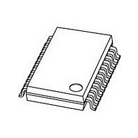
TDA8706AM NXP Semiconductors, TDA8706AM Datasheet - Page 7

TDA8706AM
Manufacturer Part Number
TDA8706AM
Description
Manufacturer
NXP Semiconductors
Datasheet
1.TDA8706AM.pdf
(17 pages)
Specifications of TDA8706AM
Number Of Elements
1
Resolution
6Bit
Sample Rate
40MSPS
Input Polarity
Unipolar
Input Type
Voltage
Rated Input Volt
0.7V
Differential Input
No
Power Supply Requirement
Analog and Digital
Single Supply Voltage (typ)
3.3V
Single Supply Voltage (min)
2.7V
Single Supply Voltage (max)
3.6V
Dual Supply Voltage (typ)
Not RequiredV
Dual Supply Voltage (min)
Not RequiredV
Dual Supply Voltage (max)
Not RequiredV
Power Dissipation
73mW
Differential Linearity Error
±0.35LSB
Integral Nonlinearity Error
±0.5LSB
Operating Temp Range
-40C to 85C
Operating Temperature Classification
Industrial
Mounting
Surface Mount
Pin Count
24
Package Type
SSOP
Input Signal Type
Single-Ended
Lead Free Status / Rohs Status
Not Compliant
Philips Semiconductors
Notes
1. In addition to a good layout of the digital and analog ground, it is recommended that the rise and fall times of the clock
2. Effective bits are derived from a Fast Fourier Transform (FFT) processing taking 2K acquisition points per equivalent
3. Output data acquisition: the output data is available after the maximum delay time t
2003 Jul 21
SYMBOL
t
t
Analog signal processing
L
INL
DNL
E
EB
Timing (f
O
t
t
t
S
t
t
t
t
t
t
r
f
ds
h
d
su
r
f
over
CLPP
MH
INEARITY
FFECTIVE BITS
ELECT INPUT SIGNALS
6-bit analog-to-digital converter
with multiplexer and clamp
UTPUT DATA
must not be less than 1 ns. A sine wave with specified amplitude is also allowed.
fundamental period. The calculation takes into account all harmonics and noise up to half of the clock frequency
(NYQUIST frequency). Conversion to signal-to-noise ratio: S/N = EB
clk
clock rise time
clock fall time
integral non-linearity
differential non-linearity
effective bits
sampling delay time
output hold time
output delay time
set-up time SR, SG and
SB
rise time SR, SG and SB
fall time SR, SG and SB
RED, GREEN and BLUE
(active) overlap time with
respect to select signals
SR, SG and SB
clamp pulse time
multiplexer hold time SR,
SG and SB
= 40 MHz; C
; note 3
; note 2
PARAMETER
SR, SG, SB
L
= 10 pF); see Fig.3
AND
CLP
10% to 90%; f
LOW = 0.8 V,
HIGH = 2.0 V
90% to 10%; f
LOW = 0.8 V,
HIGH = 2.0 V
f
f
f
f
with no overlap; see Fig.3
with overlap; see Fig.4
10% to 90%
90% to 10%
see Fig.4
C
clk
clk
clk
i
= 4.43 MHz
CLP
= 40 MHz; ramp input
= 40 MHz; ramp input
= 40 MHz;
= 10 nF
CONDITIONS
clk
clk
7
40 MHz;
40 MHz;
5.5
6.5
10
4
4
0
9
MIN.
6.02 + 1.76 dB.
5.8
9.0
12
6
6
3
0.20
0.10
d
TYP.
.
7
7
7
19
Product specification
0.5
0.35
TDA8706A
MAX.
ns
ns
LSB
LSB
bits
ns
ns
ns
ns
ns
ns
ns
ns
ns
UNIT
s


