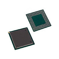
PI7C8150BND Pericom Semiconductor, PI7C8150BND Datasheet - Page 77

PI7C8150BND
Manufacturer Part Number
PI7C8150BND
Description
Manufacturer
Pericom Semiconductor
Datasheet
1.PI7C8150BND.pdf
(106 pages)
Specifications of PI7C8150BND
Operating Temperature (min)
0C
Operating Temperature Classification
Commercial
Operating Temperature (max)
85C
Package Type
BGA
Rad Hardened
No
Lead Free Status / Rohs Status
Not Compliant
Available stocks
Company
Part Number
Manufacturer
Quantity
Price
Company:
Part Number:
PI7C8150BNDE
Manufacturer:
CYPRESS
Quantity:
101
Part Number:
PI7C8150BNDE
Manufacturer:
PERICOM
Quantity:
20 000
Company:
Part Number:
PI7C8150BNDIE
Manufacturer:
PERICOM
Quantity:
300
Company:
Part Number:
PI7C8150BNDIE
Manufacturer:
PERICOM
Quantity:
301
Part Number:
PI7C8150BNDIE
Manufacturer:
PERICOM
Quantity:
20 000
14.1.14
14.1.15
14.1.16
I/O BASE REGISTER – OFFSET 1Ch
I/O LIMIT REGISTER – OFFSET 1Ch
SECONDARY STATUS REGISTER – OFFSET 1Ch
Bit
31:24
Bit
3:0
7:4
Bit
11:8
15:12
Bit
20:16
21
22
23
24
Function
Secondary
Latency Timer
Function
32-bit Indicator
I/O Base Address
[15:12]
Function
32-bit Indicator
I/O Base Address
[15:12]
Function
Reserved
66MHz Capable
Reserved
Fast Back-to-
Back Capable
Master Data
Parity Error
Detected
Type
R/W
Type
R/O
R/W
Type
R/O
R/W
Type
R/O
R/O
R/O
R/O
R/WC
Description
Designated in units of PCI bus clocks. Latency timer checks for
master accesses on the secondary bus interfaces that remain
unclaimed by any target.
Reset to 0
Description
Read as 01h to indicate 32-bit I/O addressing
Defines the bottom address of the I/O address range for the bridge
to determine when to forward I/O transactions from one interface to
the other. The upper 4 bits correspond to address bits [15:12] and
are writable. The lower 12 bits corresponding to address bits [11:0]
are assumed to be 0. The upper 16 bits corresponding to address
bits [31:16] are defined in the I/O base address upper 16 bits address
register
Reset to 0
Description
Read as 01h to indicate 32-bit I/O addressing
Defines the top address of the I/O address range for the bridge to
determine when to forward I/O transactions from one interface to
the other. The upper 4 bits correspond to address bits [15:12] and
are writable. The lower 12 bits corresponding to address bits [11:0]
are assumed to be FFFh. The upper 16 bits corresponding to
address bits [31:16] are defined in the I/O base address upper 16 bits
address register
Reset to 0
Description
Reset to 0
Set to 1 to enable 66MHz operation on the secondary interface
Reset to 1
Reset to 0
Set to 1 to enable decoding of fast back-to-back transactions on the
secondary interface to different targets
Reset to 0
Set to 1 when S_PERR_L is asserted and bit 6 of command register
is set
Reset to 0
67
March 19, 2003 – Revision 1.04
2-PORT PCI-TO-PCI BRIDGE
ADVANCE INFORMATION
PI7C8150


